|
National Semiconductor Corp
Date
Code: 9112
|
-
 Freelance Stock:
113
Freelance Stock:
113
Ships Immediately
|
|
|
National Semiconductor Corp
|
-
Freelance Stock:
35
Ships Immediately
|
|
|
National Semiconductor Corp
Date
Code: 9052
|
-
Freelance Stock:
128
Ships Immediately
|
|
|
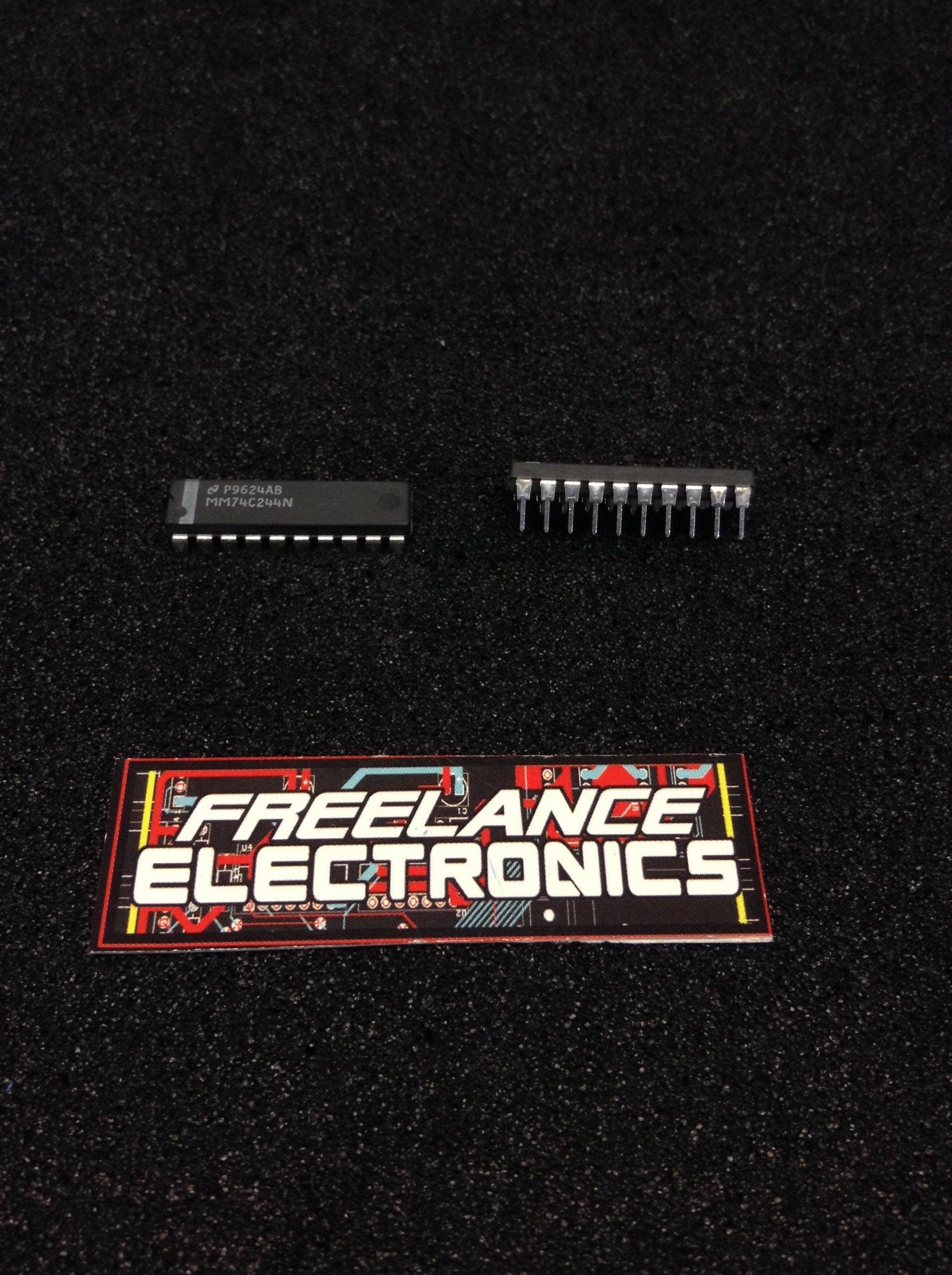
National Semiconductor Corp
Date
Code: 9624
|
-
Freelance Stock:
2
Ships Immediately
|
|
|
National Semiconductor Corp
Date
Code: 8424
|
-
Freelance Stock:
36
Ships Immediately
|
|
|
National Semiconductor Corp
Date
Code: 9024
|
-
Freelance Stock:
16
Ships Immediately
|
|
|
National Semiconductor Corp
Date
Code: 8424
|
-
Freelance Stock:
36
Ships Immediately
|
|
|
National Semiconductor Corp
Date
Code: 9624
|
-
Freelance Stock:
1
Ships Immediately
|
|
|
National Semiconductor Corp
Date
Code: 9042
|
-
Freelance Stock:
36
Ships Immediately
|
|