Closed Dec 25th-26th
800-300-1968
We Stock Hard to Find Parts
My Account
|
My Orders
|
My Cart
Questions?
(800) 300-1968
Register
(current)
My Account
(current)
My Orders
(current)
My Cart
(current)
Categories
(current)
Manufacturers
Request a Quote
Sell Your Excess
Consignment
Quality Assurance
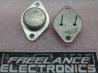
MC7815ACD2T
Part #
MC7815ACD2T
Description
IC REG LDO 15V 1A D2PAK
Category
IC
Availability
In Stock
Qty
289
Qty
Price
1 - 60
$0.95468
61 - 121
$0.75940
122 - 182
$0.71601
183 - 242
$0.66538
243 +
$0.59306
Manufacturer
Available
Qty
Motorola Corp
Freelance Stock:
5
Ships Immediately
Motorola Corp
Date Code: 0019
Freelance Stock:
50
Ships Immediately
ON Semiconductor
Date Code: 0044
Freelance Stock:
200
Ships Immediately
ON Semiconductor
Freelance Stock:
34
Ships Immediately
Add to Cart
Related Items
Motorola Corp
IC
MC7815CK
$11.25051
Motorola Corp
IC
MC7818CT
$0.61140
ON Semiconductor
RECTIFIER
MC7812ACT
$1.52063
Motorola Corp
RECTIFIER
MC7812BT
$0.35615
Motorola Corp
VOLTAGE REGULAT
MC7812CK
$23.02385
Motorola Corp
TRANSISTOR
MC7812CT
$0.30134