Closed Dec 25th-26th
800-300-1968
We Stock Hard to Find Parts
My Account
|
My Orders
|
My Cart
Questions?
(800) 300-1968
Register
(current)
My Account
(current)
My Orders
(current)
My Cart
(current)
Categories
(current)
Manufacturers
Request a Quote
Sell Your Excess
Consignment
Quality Assurance
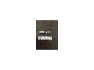
MC74AC05D
Part #
MC74AC05D
Description
BFFR/DRVR 6CH INV OPEN DRAINCMOS 14SOIC - Rail/Tube
Category
IC
Availability
Out of Stock
Qty
0
Qty
Price
1 +
$0.07827
Related Items
Motorola Corp
IC
MC74AC00D
$0.20475
ON Semiconductor
IC
MC74AC00DR2
$0.20475
Motorola Corp
IC
MC74AC00N
$0.08218
Motorola Corp
IC
MC74AC02N
$0.13176
Motorola Corp
IC
MC74AC04D
$0.08218
Motorola Corp
IC
MC74AC04DR2
$0.05868