Closed Dec 25th-26th
800-300-1968
We Stock Hard to Find Parts
My Account
|
My Orders
|
My Cart
Questions?
(800) 300-1968
Register
(current)
My Account
(current)
My Orders
(current)
My Cart
(current)
Categories
(current)
Manufacturers
Request a Quote
Sell Your Excess
Consignment
Quality Assurance
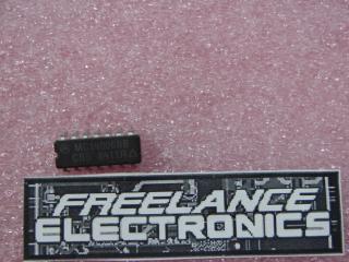
MC14093BDG
Part #
MC14093BDG
Description
LOG CMOS SCHMITT TRG QUAD - Rail/Tube
Category
IC
Availability
Out of Stock
Qty
0
Qty
Price
1 +
$0.07954
Related Items
Motorola Corp
IC
MC14000UBCL
$0.14612
Motorola Corp
IC
MC14001BCL
$2.28582
Motorola Corp
IC
MC14001BCP
$7.92777
Motorola Corp
IC
MC14002BAL
$1.09583
Motorola Corp
IC
MC14002BCP
$0.99908
Motorola Corp
IC
MC14006BBCBS
$18.10689