Closed Dec 25th-26th
800-300-1968
We Stock Hard to Find Parts
My Account
|
My Orders
|
My Cart
Questions?
(800) 300-1968
Register
(current)
My Account
(current)
My Orders
(current)
My Cart
(current)
Categories
(current)
Manufacturers
Request a Quote
Sell Your Excess
Consignment
Quality Assurance
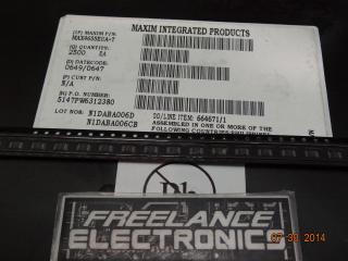
MAX4636EUB
Part #
MAX4636EUB
Description
FAST, LOW-VOLTAGE, DUAL 4 OHMSPDT CMOS ANALO - Bulk
Category
IC
Availability
Out of Stock
Qty
0
Qty
Price
1 +
$1.26026
Related Items
MAXIM
IC
MAX4614CPD
$12.78796
MAXIM
IC
MAX4622EPE
$4.10546
MAXIM
IC
MAX4632ESE
$4.28547
MAXIM
IC
MAX4638EUE
$9.06919
MAXIM
IC
MAX4655EUA
$3.06174
MAXIM
IC
MAX4655EUA+T
$1.68284