RECEIVER SECTION
ELECTRICAL CHARACTERISTICS
SWITCHING CHARACTERISTICS
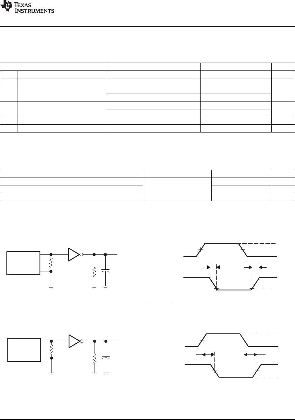
PARMETER MEASUREMENT INFORMATION
50 Ω
TEST CIRCUIT VOLTAGE WAVEFORMS
0 V
3 V
Output
Input
V
OL
V
OH
t
TLH
Generator
(see Note B)
R
L
RS-232
Output
t
THL
C
L
(see Note A)
SR(tr) +
6 V
t
THL
or t
TLH
1.5 V 1.5 V
3 V
−3 V
3 V
−3 V
TEST CIRCUIT VOLTAGE WAVEFORMS
0 V
3 V
Output
Input
V
OL
V
OH
t
PLH
t
PHL
50%
50%
1.5 V 1.5 V
50 Ω
Generator
(see Note B)
R
L
RS-232
Output
C
L
(see Note A)
MAX3232-EP
www.ti.com
......................................................................................................................................................... SGLS337A – APRIL 2006 – REVISED MARCH 2009
over recommended ranges of supply voltage and operating free-air temperature (unless otherwise noted (see
(1)
and Figure 4 )
PARAMETER TEST CONDITIONS MIN TYP
(2)
MAX UNIT
V
OH
High -level output voltage I
OH
= -1 mA V
CC
– 0.6 V
CC
– 0.1 V
V
OL
Low -level output voltage I
OL
= 1.6 mA 0.4 V
V
CC
= 3.3 V 1.5 2.4
V
IT+
Positive -going input threshold voltage V
V
CC
= 5 V 1.8 2.4
V
CC
= 3.3 V 0.6 1.2
V
IT –
Negative -going input threshold voltage V
V
CC
= 5 V 0.8 1.5
V
hys
Input hysteresis (V
IT+
– V
IT –
) 0.3 V
r
i
Input resistance V
I
= ± 3 V to ± 25 V 3 5 8 k Ω
(1) Test conditions are C1 – C4 = 0.1 µ F at V
CC
= 3.3 V ± 0.3 V; C1 = 0.047 µ F, C2 – C4 = 0.33 µ F at V
CC
= 5 V ± 0.5 V.
(2) All typical values are at V
CC
= 3.3 V or V
CC
= 5 V and T
A
= 25 ° C.
over recommended ranges of supply voltage and operating free-air temperature (unless otherwise noted (see
(1)
and Figure 3 )
PARAMETER TEST CONDITIONS MIN TYP
(2)
MAX UNIT
t
PLH
Propagation delay time, low - to high -level output 300 ns
C
L
= 150 pF
t
PHL
Propagation delay time, high - to low -level output 300 ns
t
sk(p)
Pulse skew
(3)
300 ns
(1) Test conditions are C1 – C4 = 0.1 µ F at V
CC
= 3.3 V ± 0.3 V; C1 = 0.047 µ F, C2 – C4 = 0.33 µ F at V
CC
= 5 V ± 0.5 V.
(2) All typical values are at V
CC
= 3.3 V or V
CC
= 5 V and T
A
= 25 ° C.
(3) Pulse skew is defined as |t
PLH
– t
PHL
| of each channel of the same device.
Figure 1. Driver Slew Rate
A. C
L
includes probe and jig capacitance.
B. The pulse generator has the following characteristics: Z
O
= 50 Ω , 50% duty cycle, tr ≤ 10 ns, tf ≤ 10 ns.
Figure 2. Driver Pulse Skew
Copyright © 2006 – 2009, Texas Instruments Incorporated Submit Documentation Feedback 5
Product Folder Link(s): MAX3232-EP


