Freelance Electronics Components Distributor
Closed Dec 25th-26th
800-300-1968
We Stock Hard to Find Parts

MAX1204BCAP

Part # MAX1204BCAP
Description IC ADC 8CH 10BIT 133KHZ 20-SSOP
Category IC
Availability In Stock
Qty 1
Qty Price
1 + $6.32682
Manufacturer Available Qty
MAXIM
Date Code: 9708
  • Shipping Freelance Stock: 1
    Ships Immediately


Technical Document


DISCLAIMER: The information provided herein is solely for informational purposes. Customers must be aware of the suitability of this product for their application, and consider that variable factors such as Manufacturer, Product Category, Date Codes, Pictures and Descriptions may differ from available inventory.

_______________General Description
The MAX1204 is a 10-bit data-acquisition system
specifically designed for use in applications with mixed
+5V (analog) and +3V (digital) supply voltages. It oper-
ates with a single +5V analog supply or dual ±5V ana-
log supplies, and combines an 8-channel multiplexer,
internal track/hold, and serial interface with high con-
version speed and low power consumption.
A 4-wire serial interface connects directly to
SPI™/Microwire™ devices without external logic, and a
serial strobe output allows direct connection to
TMS320-family digital signal processors. The MAX1204
uses either the internal clock or an external serial-
interface clock to perform successive-approximation
analog-to-digital conversions. The serial interface oper-
ates at up to 2MHz.
The MAX1204 features an internal 4.096V reference and
a reference-buffer amplifier that simplifies gain trim. It
also has a VL pin that supplies power to the digital out-
puts. Output logic levels (3V, 3.3V, or 5V) are determined
by the value of the voltage applied to this pin.
A hard-wired SHDN pin and two software-selectable
power-down modes are provided. Accessing the serial
interface automatically powers up the device. A quick
turn-on time allows the MAX1204 to be shut down
between conversions, enabling the user to optimize
supply currents. By customizing power-down between
conversions, supply current can drop below 10µA at
reduced sampling rates.
The MAX1204 is available in 20-pin SSOP and DIP
packages, and is specified for the commercial, extend-
ed, and military temperature ranges.
________________________Applications
5V/3V Mixed-Supply Systems
Data Acquisition
Process Control
Battery-Powered Instruments
Medical Instruments
____________________________Features
8-Channel Single-Ended or 4-Channel
Differential Inputs
Operates from +5V Single or ±5V Dual Supplies
User-Adjustable Output Logic Levels
(2.7V to 5.25V)
Low Power: 1.5mA (operating mode)
2µA (power-down mode)
Internal Track/Hold, 133kHz Sampling Rate
Internal 4.096V Reference
SPI/Microwire/TMS320-Compatible
4-Wire Serial Interface
Software-Configurable Unipolar/Bipolar Inputs
20-Pin DIP/SSOP
Pin-Compatible 12-Bit Upgrade: MAX1202
MAX1204
5V, 8-Channel, Serial, 10-Bit ADC
with 3V Digital Interface
________________________________________________________________
Maxim Integrated Products
1
20
19
18
17
16
15
14
13
12
11
1
2
3
4
5
6
7
8
9
10
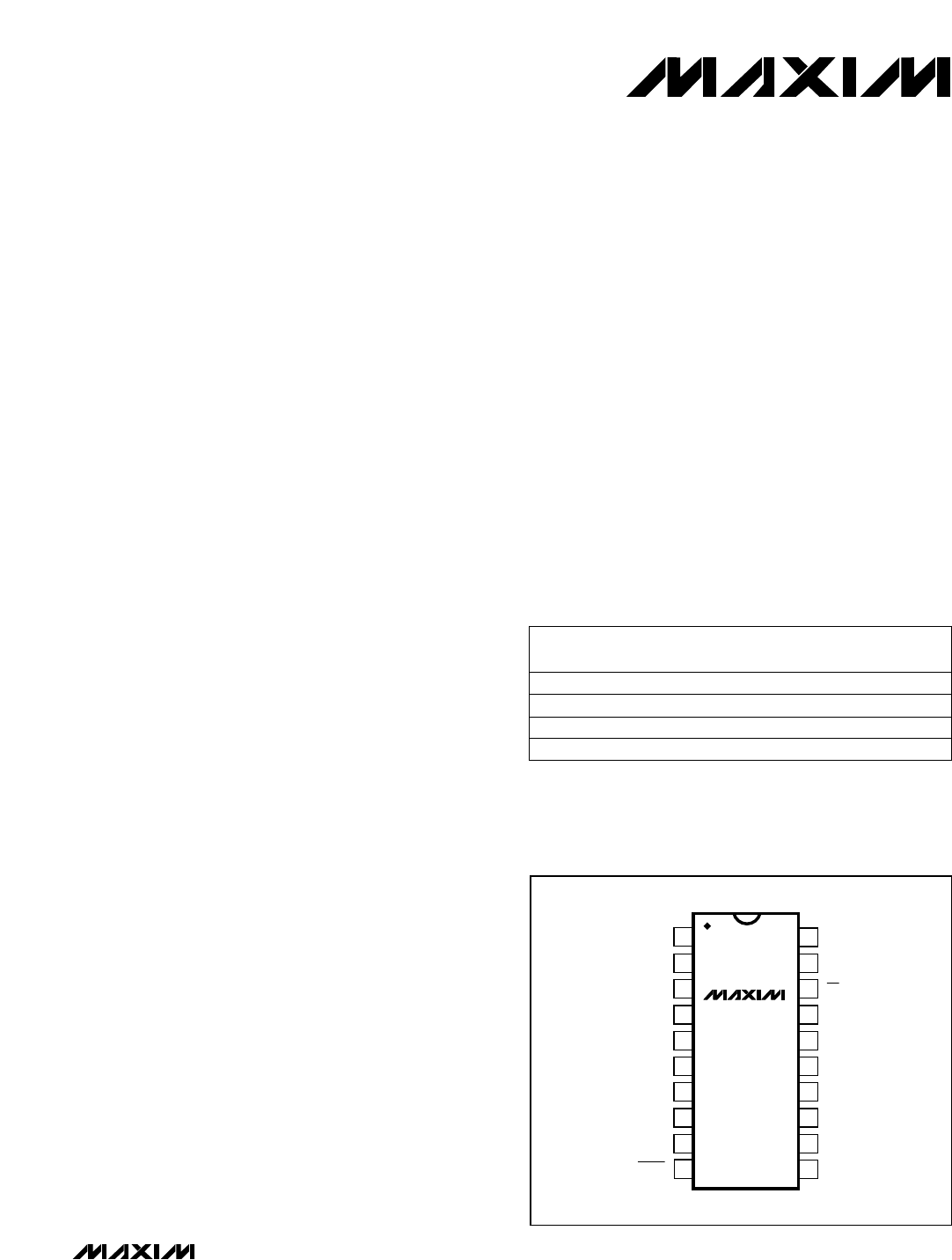
TOP VIEW
DIP/SSOP
V
DD
SCLK
CS
DIN
SSTRB
DOUT
VL
GND
REFADJ
REFSHDN
V
SS
CH7
CH6
CH5
CH4
CH3
CH2
CH1
CH0
MAX1204
__________________Pin Configuration
19-1179; Rev 0; 1/97
______________Ordering Information
For free samples & the latest literature: http://www.maxim-ic.com, or phone 1-800-998-8800
Typical Operating Circuit appears on last page.
SPI is a registered trademark of Motorola, Inc.
Microwire is a registered trademark of National Semiconductor Corp.
Ordering Information continued at end of data sheet.
PART
MAX1204ACPP
MAX1204BCPP
MAX1204ACAP 0°C to +70°C
0°C to +70°C
0°C to +70°C
TEMP. RANGE PIN-PACKAGE
20 Plastic DIP
20 Plastic DIP
20 SSOP
MAX1204BCAP 0°C to +70°C 20 SSOP
INL
(LSB)
±1/2
±1
±1/2
±1
MAX1204
5V, 8-Channel, Serial, 10-Bit ADC
with 3V Digital Interface
2 _______________________________________________________________________________________
ABSOLUTE MAXIMUM RATINGS
Stresses beyond those listed under “Absolute Maximum Ratings” may cause permanent damage to the device. These are stress ratings only, and functional
operation of the device at these or any other conditions beyond those indicated in the operational sections of the specifications is not implied. Exposure to
absolute maximum rating conditions for extended periods may affect device reliability.
V
DD
to GND..............................................................-0.3V to +6V
VL ...............................................................-0.3V to (V
DD
+ 0.3V)
V
SS
to GND...............................................................+0.3V to -6V
V
DD
to V
SS
..............................................................-0.3V to +12V
CH0–CH7 to GND............................(V
SS
- 0.3V) to (V
DD
+ 0.3V)
CH0–CH7 Total Input Current...........................................±20mA
REF to GND................................................-0.3V to (V
DD
+ 0.3V)
REFADJ to GND .........................................-0.3V to (V
DD
+ 0.3V)
Digital Inputs to GND .................................-0.3V to (V
DD
+ 0.3V)
Digital Outputs to GND.................................-0.3V to (VL + 0.3V)
Digital Output Sink Current .................................................25mA
Continuous Power Dissipation (T
A
= +70°C)
Plastic DIP (derate 11.11mW/°C above +70°C) ...........889mW
SSOP (derate 8.00mW/°C above +70°C) .....................640mW
CERDIP (derate 11.11mW°C above +70°C).................889mW
Operating Temperature Ranges
MAX1204_C_P .....................................................0°C to +70°C
MAX1204_E_P ..................................................-40°C to +85°C
MAX1204BMJP...............................................-55°C to +125°C
Storage Temperature Range .............................-60°C to +150°C
ELECTRICAL CHARACTERISTICS
(V
DD
= +5V ±5%, VL = 2.7V to 3.6V; V
SS
= 0V or -5V ±5%; f
SCLK
= 2.0MHz, external clock (50% duty cycle); 15 clocks/conversion
cycle (133ksps); 4.7µF capacitor at REF; T
A
= T
MIN
to T
MAX
; unless otherwise noted.)
MAX1204A
V
IN
= 4.096Vp-p, 65kHz (Note 4)
External reference, 4.096V
MAX1204B
No missing codes over temperature
MAX1204A
MAX1204B
CONDITIONS
dB-75Channel-to-Channel Crosstalk
dB70SFDRSpurious-Free Dynamic Range
dB-70THD
Total Harmonic Distortion
(up to the 5th harmonic)
dB66SINADSignal-to-Noise + Distortion Ratio
LSB
±0.5
INLRelative Accuracy (Note 2)
Bits10Resolution
LSB±0.1
Channel-to-Channel
Offset Matching
ppm/°C±0.8Gain Temperature Coefficient
±1.0
LSB±1.0DNLDifferential Nonlinearity
LSB
±1.0
Offset Error
±2.0
UNITSMIN TYP MAXSYMBOLPARAMETER
-3dB rolloff MHz4.5Small-Signal Bandwidth
kHz800Full-Power Bandwidth
LSB
±1.0
Gain Error (Note 3)
±2.0
MAX1204A
MAX1204B
DC ACCURACY (Note 1)
DYNAMIC SPECIFICATIONS (10kHz sine-wave input, 4.096Vp-p, 133ksps, 2.0MHz external clock, bipolar input mode)
MAX1204
5V, 8-Channel, Serial, 10-Bit ADC
with 3V Digital Interface
_______________________________________________________________________________________ 3
ELECTRICAL CHARACTERISTICS (continued)
(V
DD
= +5V ±5%, VL = 2.7V to 3.6V; V
SS
= 0V or -5V ±5%; f
SCLK
= 2.0MHz, external clock (50% duty cycle); 15 clocks/conversion
cycle (133ksps); 4.7µF capacitor at REF; T
A
= T
MIN
to T
MAX
; unless otherwise noted.)
MAX1204AC
T
A
= +25°C
External clock, 2MHz, 12 clocks/conversion
(Note 6)
On/off leakage current, V
CH_
= ±5V
Bipolar, V
SS
= -5V
Unipolar, V
SS
= 0V
6
Used for data transfer only
Internal compensation mode (Note 6)
Internal clock
External compensation mode, 4.7µF
CONDITIONS
ppm/°C
±30 ±50
V
REF
Temperature Coefficient
mA30REF Short-Circuit Current
V4.076 4.096 4.116REF Output Voltage
pF16Input Capacitance
µA±0.01 ±1Multiplexer Leakage Current
±V
REF
/2
V
V
REF
Input Voltage Range, Single-
Ended and Differential (Note 7)
0 2.0
0.1 0.4 MHz
0.1 2.0
External Clock-Frequency Range
MHz1.7Internal Clock Frequency
ns10Aperture Delay
µs1.5t
ACQ
Track/Hold Acquisition Time
µs
5.5 10
t
CONV
Conversion Time (Note 5)
UNITSMIN TYP MAXSYMBOLPARAMETER
MAX1204AE ±30 ±60
±30MAX1204B
0mA to 0.5mA output load mV2.5Load Regulation (Note 8)
Internal compensation mode
µF
0
Capacitive Bypass at REF
External compensation mode 4.7
µF0.01Capacitive Bypass at REFADJ
%±1.5REFADJ Adjustment Range
V
2.50 V
DD
+
50mV
Input Voltage Range
µA200 350Input Current
k
12 20Input Resistance
SHDN = 0V
µA1.5 10REF Input Current in Shutdown
V
V
DD
-
50mV
REFADJ Buffer Disable Threshold
ps<50Aperture Jitter
CONVERSION RATE
INTERNAL REFERENCE
ANALOG INPUT
EXTERNAL REFERENCE AT REF (Buffer disabled, V
REF
= 4.096V)
1234567NEXT