Closed Dec 25th-26th
800-300-1968
We Stock Hard to Find Parts
My Account
|
My Orders
|
My Cart
Questions?
(800) 300-1968
Register
(current)
My Account
(current)
My Orders
(current)
My Cart
(current)
Categories
(current)
Manufacturers
Request a Quote
Sell Your Excess
Consignment
Quality Assurance
LTC3407EDD-2
Part #
LTC3407EDD-2
Description
IC REG BCK SYNC ADJ 0.8A 10DFN
Category
IC
Availability
In Stock
Qty
1
Qty
Price
1 +
$8.61638
Manufacturer
Available
Qty
Linear Technology
Date Code: 0552
Freelance Stock:
1
Ships Immediately
Add to Cart
Related Items
Linear Technology
IC
LTC3407AEMSE-2#TRPBF
$4.30331
Linear Technology
IC
LTC3411AIMS#TRPBF
$4.59375
Linear Technology
IC
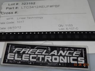
LTC3412AEUF#PBF
$9.11505
Linear Technology
IC
LTC3412EUF#TRMPBF
$4.98235
Linear Technology
IC
LTC3413EFE
$7.22115
Linear Technology
IC
LTC3413EFE#PBF
$2.72752