Closed Dec 25th-26th
800-300-1968
We Stock Hard to Find Parts
My Account
|
My Orders
|
My Cart
Questions?
(800) 300-1968
Register
(current)
My Account
(current)
My Orders
(current)
My Cart
(current)
Categories
(current)
Manufacturers
Request a Quote
Sell Your Excess
Consignment
Quality Assurance
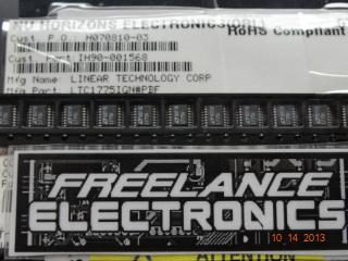
LTC1727ES8-5
Part #
LTC1727ES8-5
Description
IC MON TRPL SPPLY MICROPWR 8SOIC
Category
IC
Availability
In Stock
Qty
5
Qty
Price
1 +
$4.66482
Manufacturer
Available
Qty
Linear Technology
Date Code: 9205
Freelance Stock:
5
Ships Immediately
Add to Cart
Related Items
Linear Technology
IC
LTC17351S-1
Linear Technology
IC
LTC1746IFW
$20.97417
Linear Technology
IC
LTC1775IGN#PBF
$9.86121
Linear Technology
VOLTAGE REGULAT
LTC1754ES6-5#TRMPBF
$2.05034
Fairchild Semiconductor
IC
008-25424
$11.58351
Harris Corporation
IC
01-6945-9