Closed Dec 25th-26th
800-300-1968
We Stock Hard to Find Parts
My Account
|
My Orders
|
My Cart
Questions?
(800) 300-1968
Register
(current)
My Account
(current)
My Orders
(current)
My Cart
(current)
Categories
(current)
Manufacturers
Request a Quote
Sell Your Excess
Consignment
Quality Assurance
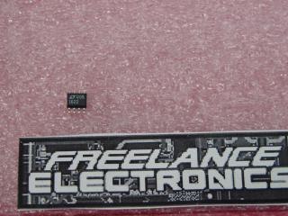
LTC1688CS
Part #
LTC1688CS
Description
IC DVR 100MBPS RS485 QUAD 16SOIC
Category
IC
Availability
Out of Stock
Qty
0
Qty
Price
1 +
$11.94731
Related Items
Linear Technology
IC
LTC1605-1CG
$30.36032
Generic
IC
LTC1622CS8
$2.32484
Linear Technology
IC
LTC1642CGN
$3.94445
Linear Technology
IC
LTC1665CGN#PBF
$9.04121
Linear Technology
IC
LTC1669CS#TRMPBF
$8.91038
Linear Technology
IC
LTC1690IS8
$5.89240