Closed Dec 25th-26th
800-300-1968
We Stock Hard to Find Parts
My Account
|
My Orders
|
My Cart
Questions?
(800) 300-1968
Register
(current)
My Account
(current)
My Orders
(current)
My Cart
(current)
Categories
(current)
Manufacturers
Request a Quote
Sell Your Excess
Consignment
Quality Assurance
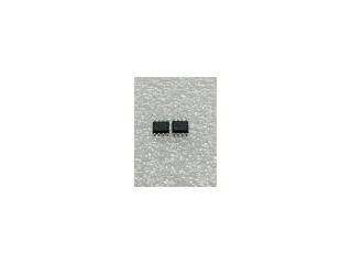
LT1461DHS8-4
Part #
LT1461DHS8-4
Description
IC VREF SERIES 4.096V 8SOIC
Category
IC
Availability
Out of Stock
Qty
0
Qty
Price
1 +
$4.47423
Related Items
Linear Technology
IC
LT1461AIS8-5#PBF
$8.02780
Linear Technology
IC
LT1461CCS8-3.3#PBF
$1.48756
Linear Technology
IC
LT1462CS8#PBF
$2.90760
Fairchild Semiconductor
IC
008-25424
$11.58351
Harris Corporation
IC
01-6945-9
Motorola Corp
IC
010-143121-0002