Freelance Electronics Components Distributor
Closed Dec 25th-26th
800-300-1968
We Stock Hard to Find Parts

LT1431CN8

Part # LT1431CN8
Description V-Ref Adjustable 2.5V to 36V100mA 8-Pin PDIP N
Category IC
Availability In Stock
Qty 18
Qty Price
1 - 3 $5.14448
4 - 7 $4.09220
8 - 11 $3.85836
12 - 15 $3.58554
16 + $3.19581
Manufacturer Available Qty
Linear Technology
Date Code: 9229
  • Shipping Freelance Stock: 8
    Ships Immediately
Linear Technology
Date Code: 9400
  • Shipping Freelance Stock: 10
    Ships Immediately


Technical Document


DISCLAIMER: The information provided herein is solely for informational purposes. Customers must be aware of the suitability of this product for their application, and consider that variable factors such as Manufacturer, Product Category, Date Codes, Pictures and Descriptions may differ from available inventory.

4
LT1431
CCHARA TERIST
ICS
UW
AT
Y
P
I
CA
LPER
F
O
R
C
E
FREQUENCY (Hz)
20
REF-TO-COLL 1k LOAD A
V
(dB)
40
80
120
140
100 10k 100k 10M
LT1431 • TPC08
0
1k
1M
100
60
–20
–90
–45
45
135
180
–135
90
0
180
PHASE (DEG)
PHASE
A
V
Voltage Gain and Phase
vs Frequency
FREQUENCY (Hz)
10
10
100 10k 100k 10M
LT1431 • TPC09
1k 1M
–90
–45
45
135
180
–135
90
0
180
PHASE (DEG)
10
9
10
8
10
7
10
6
10
5
10
4
10
3
10
2
REF-TO-COLL gm (m )
PHASE
gm
Transconductance and Phase
vs Frequency (REF to COLL)
Transconductance and Phase vs
Frequency (Ref to Comp)
Dynamic Impedance vs Frequency
TEMPERATURE (˚C)
–50
V
COMP
(V)
2.0
2.5
3.0
25 75
LT1431 • TPC12
1.5
1.0
–25 0
50 100 125
0.5
0
I
COLL
= 100mA
I
COLL
= 10mA
V
COMP
vs Temperature vs I
COLL
I
COMP
vs V
COMP
vs V
REF
Noise vs Frequency 0.1Hz to 10Hz Noise
FREQUENCY (Hz)
NOISE (nV/Hz)
1000
1 100 1k 100k
LT1431 • G14
10 10k
500
0
TIME (MINUTES)
0
35
LT1431 • TPC15
12
46
NOISE VOLTAGE (50µV/DIV)
FREQUENCY (Hz)
10
4
100 10k 100k 10M
LT1431 • TPC10
1k 1M
100
–80
–40
0
20
120
–20
–60
140
PHASE (DEG)
3 × 10
3
10
3
0.1
REF-TO-COLL gm (µ )
PHASE
gm
3 × 10
2
FREQUENCY (Hz)
100
0.8
1.0
1.2
1.4
1k 10k 100k
LT1431 • TPC11
0.6
0.4
0.2
0
I
K
100mA
Z
KA
()
V
COMP
(V)
0
I
COMP
(µA)
400
500
600
1.5 2.5
LT1431 • TPC13
300
200
0.5 1.0
2.0 3.0 3.5
100
0
V
REF
= 5V
V
REF
= 4V
V
REF
= 3V
V
REF
= 2.53V
5
LT1431
PI FU CTIO S
U
UU
COLL (Pin 1): Open collector of the output transistor. The
maximum pin voltage is 26V. The saturation voltage at
100mA is approximately 1V.
COMP (Pin 2): Base of the driver for the output transistor.
This pin allows additional compensation for complex
feedback systems and shutdown of the regulator. It must
be left open if unused.
V
+
(Pin 3): Bias voltage for the entire shunt regulator. The
maximum input voltage is 36V and the minimum to
operate is equal to V
REF
(2.5V). The quiescent current is
typically 0.6mA.
R
TOP
(Pin 4): Top of the on-chip 5k-5k resistive divider
that guarantees 1% accuracy of operation as a 5V shunt
regulator with no external trim. The pin is tied to COLL for
self-contained 5V operation. It may be left open if unused.
See note on parasitic diodes below.
GND-S (Pin 5): Ground reference for the on-chip resistive
divider and shunt regulator circuitry except for the output
transistor. This pin allows external current limit of the
output transistor with one resistor between GND-F (force)
and GND-S (sense).
GND-F (Pin 6): Emitter of the output transistor and sub-
strate connection for the die.
R
MID
(Pin 7): Middle of the on-chip resistive divider string
between R
TOP
and GND-S. The pin is tied to REF for self-
contained 5V operation. It may be left open if unused.
REF (Pin 8): Control pin of the shunt regulator with a 2.5V
threshold. If V
+
> 3V, input bias current cancellation
reduces I
B
to 0.2µA typical.
COMP, R
TOP
, R
MID
, and REF have static discharge protec-
tion circuits that must not be activated on a continuous
basis. Therefore, the absolute maximum DC voltage on
these pins is 6V, well beyond the normal operating condi-
tions.
As with all bipolar ICs, the LT1431 contains parasitic
diodes which must not be forward biased or else anoma-
lous behavior will result. Pin conditions to be avoided are
R
TOP
below R
MID
in voltage and any pin below GND-F in
voltage (except for GND-S).
The following pin definitions apply to the Z package.
CATHODE (Pin 1): Corresponds to COLL and V
+
tied
together.
ANODE (Pin 2): Corresponds to GND-S and GND-F tied
together.
REF (Pin 3): Corresponds to REF.
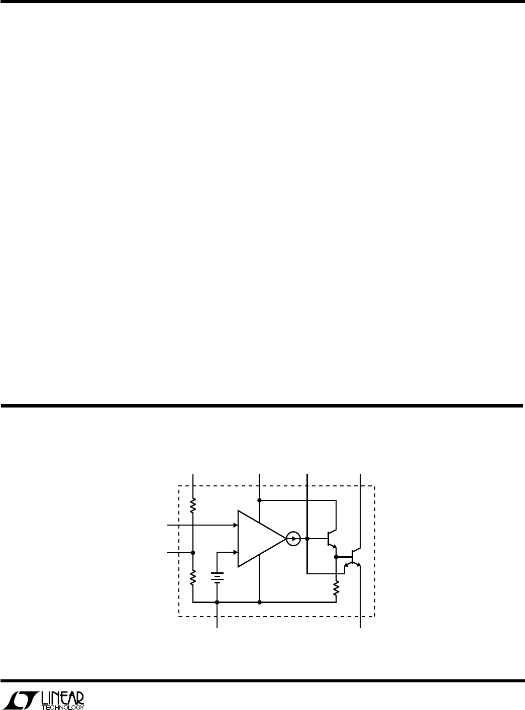
W
IDAGRA
B
L
O
C
K
LT1431 • BD01
COMPV
+
GND-FORCE
GND-SENSE
R
TOP
REF
R
MID
2.5V
+
gm = 
4mA/V
5k
COLLECTOR
8
7
5
4321
6
5k
6
LT1431
APPLICATIO S I FOR ATIO
UU W U
Frequency Compensation
As a shunt regulator, the LT1431 is stable for all capacitive
loads on the COLL pin. Capacitive loading between 0.01µF
and 18µF causes reduced phase margin with some ringing
under transient conditions. Output capacitors should not
be used arbitrarily because output noise is not necessarily
reduced.
Excess capacitance on the REF pin can introduce enough
phase shift to induce oscillation when configured as a
reference >2.5V. This can be compensated with capaci-
tance between COLL and REF (phase lead). More compli-
cated feedback loops may require shaping of the fre-
quency response of the LT1431 with dominant pole or
pole-zero compensation. This can be accomplished with a
capacitor or series resistor and capacitor between COLL
and COMP.
The compensation schemes mentioned above use voltage
feedback to stabilize the circuits. There must be voltage
gain at the COLL pin for them to be effective, so the COLL
pin must see a reasonable AC impedance. Capacitive
loading of the COLL pin reduces the AC impedance,
voltage gain, and frequency response, thereby decreasing
the effectiveness of the compensation schemes, but also
decreasing their necessity.
V
IN
R
L
2.5V
LT1431 • TA02
CATHODE
REF
LT1431Z
ANODE
V
IN
R
L
2.5V
LT1431 • TA03
COLL
REF
LT1431
GND-F
V
+
GND-S
2.5V Reference
3-Pin Package
2.5V Reference
8-Pin Package 5V Reference
Increasing 5V Reference
Programmable Reference with Adjustable
Current Limit
TYPICAL APPLICATIO S
U
V
IN
R
L
5V
LT1431 • TA04
COLL
REF
LT1431
GND-F
V
+
GND-S
R
TOP
R
MID
V
IN
R
L
5V +
LT1431 • TA05
R
= R × (0.5mA) ±25% PROCESS TOLERANCE
500mV
COLL
REF
LT1431
GND-F
V
+
GND-S
R
TOP
R
MID
V
IN
R
L
LT1431 • TA06
R
LIM
V
OUT
=
()
1 +
R1
R2
V
REF
R1
R2
I
LIMIT
=
0.7
R
LIM
+ 3.6
AT 25°C
COLL
REF
LT1431
GND-F
V
+
GND-S
PREVIOUS1234NEXT