Closed Dec 25th-26th
800-300-1968
We Stock Hard to Find Parts
My Account
|
My Orders
|
My Cart
Questions?
(800) 300-1968
Register
(current)
My Account
(current)
My Orders
(current)
My Cart
(current)
Categories
(current)
Manufacturers
Request a Quote
Sell Your Excess
Consignment
Quality Assurance
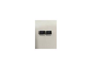
LT1054CP
Part #
LT1054CP
Description
SWTH CAPACITOR V/CONVERTER W/REGULATORS - Rail/Tube
Category
IC
Availability
Out of Stock
Qty
0
Qty
Price
1 +
$0.94397
Related Items
Linear Technology
IC
LT1054CN8
$2.16569
Linear Technology
IC
LT1054CNB
Linear Technology
IC
LT1054ISW
$1.03433
Linear Technology
IC
LT1057MH/883C
$120.54117
Linear Technology
IC
LT1058AML/883C
$104.46902
Linear Technology
IC
LT1058CN
$10.06245