Closed Dec 25th-26th
800-300-1968
We Stock Hard to Find Parts
My Account
|
My Orders
|
My Cart
Questions?
(800) 300-1968
Register
(current)
My Account
(current)
My Orders
(current)
My Cart
(current)
Categories
(current)
Manufacturers
Request a Quote
Sell Your Excess
Consignment
Quality Assurance
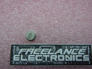
LT1032IN
Part #
LT1032IN
Description
IC LINE DRIVER LOWPWR QUAD 14DIP
Category
IC
Availability
In Stock
Qty
60
Qty
Price
1 - 12
$12.46447
13 - 25
$9.91492
26 - 37
$9.34835
38 - 50
$8.68736
51 +
$7.74308
Manufacturer
Available
Qty
Linear Technology
Date Code: 0043
Freelance Stock:
60
Ships Immediately
Add to Cart
Related Items
Linear Technology
IC
LT1032MJ
$29.91786
Linear Technology
IC
LT1032MJ/883
$59.61164
Linear Technology
IC
LT1032MJ/883C
$33.75154
Linear Technology
IC
LT1039CN
$2.09900
Linear Technology
IC
LT1039CN16
$3.67989
Linear Technology
TRANSISTOR
LT1031CCH
$10.38127