Closed Dec 25th-26th
800-300-1968
We Stock Hard to Find Parts
My Account
|
My Orders
|
My Cart
Questions?
(800) 300-1968
Register
(current)
My Account
(current)
My Orders
(current)
My Cart
(current)
Categories
(current)
Manufacturers
Request a Quote
Sell Your Excess
Consignment
Quality Assurance
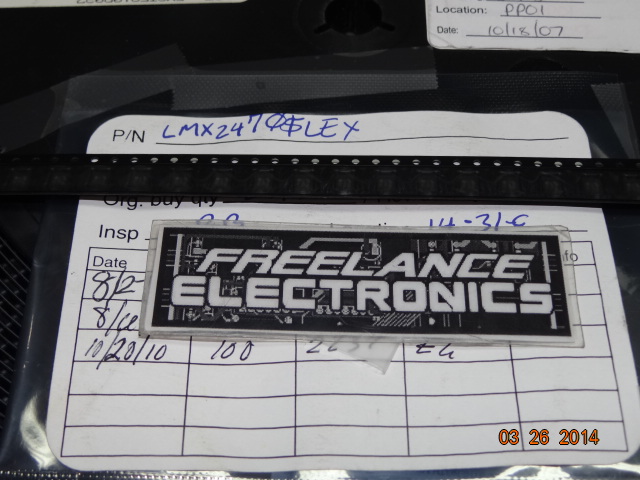
LMX2470SLEX
Part #
LMX2470SLEX
Description
IC PLL DELTA-SIGMA 24LAMUCSP
Category
IC
Availability
Out of Stock
Qty
0
Qty
Price
1 +
$1.75648
Related Items
QUALCOMM
IC
LMX24706LEX
$13.42640
National Semiconductor Corp
IC
LMX2485ESQ/NOPB
$2.11208
National Semiconductor Corp
IC
LMX2487ESQ/NOPB
$2.42691
Fairchild Semiconductor
IC
008-25424
$11.58351
Harris Corporation
IC
01-6945-9
Motorola Corp
IC
010-143121-0002