Freelance Electronics Components Distributor
Closed Dec 25th-26th
800-300-1968
We Stock Hard to Find Parts

LMC6482IMM

Part # LMC6482IMM
Description CMOS DUAL RAIL-TO-RAIL INPUTAND OUTPUT - Tape and Reel
Category IC
Availability Out of Stock
Qty 0
Qty Price
1 + $0.37305


Technical Document


DISCLAIMER: The information provided herein is solely for informational purposes. Customers must be aware of the suitability of this product for their application, and consider that variable factors such as Manufacturer, Product Category, Date Codes, Pictures and Descriptions may differ from available inventory.

LMC6482
www.ti.com
SNOS674D NOVEMBER 1997REVISED MARCH 2013
LMC6482 CMOS Dual Rail-To-Rail Input and Output Operational Amplifier
Check for Samples: LMC6482
1
FEATURES
APPLICATIONS
2
(Typical Unless Otherwise Noted)
Data Acquisition Systems
Rail-to-Rail Input Common-Mode Voltage Transducer Amplifiers
Range (Ensured Over Temperature)
Hand-held Analytic Instruments
Rail-to-Rail Output Swing (within 20mV of
Medical Instrumentation
Supply Rail, 100kΩ Load)
Active Filter, Peak Detector, Sample and Hold,
Ensured 3V, 5V and 15V Performance
pH Meter, Current Source
Excellent CMRR and PSRR: 82dB
Improved Replacement for TLC272, TLC277
Ultra Low Input Current: 20fA
High Voltage Gain (R
L
= 500kΩ): 130dB
Specified for 2kΩ and 600Ω Loads
Available in VSSOP Package
DESCRIPTION
The LMC6482 provides a common-mode range that extends to both supply rails. This rail-to-rail performance
combined with excellent accuracy, due to a high CMRR, makes it unique among rail-to-rail input amplifiers.
It is ideal for systems, such as data acquisition, that require a large input signal range. The LMC6482 is also an
excellent upgrade for circuits using limited common-mode range amplifiers such as the TLC272 and TLC277.
Maximum dynamic signal range is assured in low voltage and single supply systems by the LMC6482's rail-to-rail
output swing. The LMC6482's rail-to-rail output swing is ensured for loads down to 600Ω.
Ensured low voltage characteristics and low power dissipation make the LMC6482 especially well-suited for
battery-operated systems.
LMC6482 is also available in VSSOP package which is almost half the size of a SOIC-8 device.
See the LMC6484 data sheet for a Quad CMOS operational amplifier with these same features.
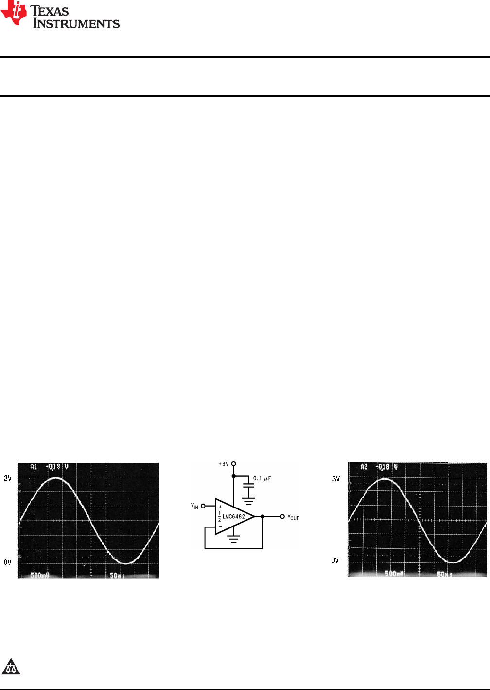
3V Single Supply Buffer Circuit
Figure 1. Rail-To-Rail Input Figure 2. Figure 3. Rail-To-Rail Output
1
Please be aware that an important notice concerning availability, standard warranty, and use in critical applications of
Texas Instruments semiconductor products and disclaimers thereto appears at the end of this data sheet.
2All trademarks are the property of their respective owners.
PRODUCTION DATA information is current as of publication date.
Copyright © 1997–2013, Texas Instruments Incorporated
Products conform to specifications per the terms of the Texas
Instruments standard warranty. Production processing does not
necessarily include testing of all parameters.
LMC6482
SNOS674D NOVEMBER 1997REVISED MARCH 2013
www.ti.com
Connection Diagram
These devices have limited built-in ESD protection. The leads should be shorted together or the device placed in conductive foam
during storage or handling to prevent electrostatic damage to the MOS gates.
Absolute Maximum Ratings
(1)(2)
ESD Tolerance
(3)
1.5kV
Differential Input Voltage ±Supply Voltage
Voltage at Input/Output Pin (V
+
) +0.3V, (V
) 0.3V
Supply Voltage (V
+
V
) 16V
Current at Input Pin
(4)
±5mA
Current at Output Pin
(5) (6)
±30mA
Current at Power Supply Pin 40mA
Lead Temperature (Soldering, 10 sec.) 260°C
Storage Temperature Range 65°C to +150°C
Junction Temperature
(7)
150°C
(1) Absolute Maximum Ratings indicate limits beyond which damage to the device may occur. Operating Ratings indicate conditions for
which the device is intended to be functional, but specific performance is not ensured. For ensured specifications and the test
conditions, see the Electrical Characteristics.
(2) If Military/Aerospace specified devices are required, please contact the TI Sales Office/Distributors for availability and specifications.
(3) Human body model, 1.5kΩ in series with 100pF. All pins rated per method 3015.6 of MIL-STD-883. This is a Class 1 device rating.
(4) Limiting input pin current is only necessary for input voltages that exceed absolute maximum input voltage ratings.
(5) Applies to both single-supply and split-supply operation. Continuous short circuit operation at elevated ambient temperature can result in
exceeding the maximum allowed junction temperature of 150°C. Output currents in excess of ±30mA over long term may adversely
affect reliability.
(6) Do not short circuit output to V
+
, when V
+
is greater than 13V or reliability will be adversely affected.
(7) The maximum power dissipation is a function of T
J(max)
, θ
JA
, and T
A
. The maximum allowable power dissipation at any ambient
temperature is P
D
= (T
J(max)
T
A
)/θ
JA
. All numbers apply for packages soldered directly into a PC board.
Operating Ratings
Supply Voltage 3.0V V+ 15.5V
Junction Temperature Range
LMC6482AM 55°C T
J
+125°C
LMC6482AI, LMC6482I 40°C T
J
+85°C
Thermal Resistance (θ
JA
)
P0008E Package, 8-Pin PDIP 90°C/W
D0008A Package, 8-Pin SOIC 155°C/W
DGK0008A Package, 8-Pin VSSOP 194°C/W
(1) Absolute Maximum Ratings indicate limits beyond which damage to the device may occur. Operating Ratings indicate conditions for
which the device is intended to be functional, but specific performance is not ensured. For ensured specifications and the test
conditions, see the Electrical Characteristics.
2 Submit Documentation Feedback Copyright © 1997–2013, Texas Instruments Incorporated
Product Folder Links: LMC6482
LMC6482
www.ti.com
SNOS674D NOVEMBER 1997REVISED MARCH 2013
DC Electrical Characteristics
Unless otherwise specified, all limits specified for T
J
= 25°C, V
+
= 5V, V
= 0V, V
CM
= V
O
= V
+
/2 and R
L
> 1M. Boldface limits
apply at the temperature extremes.
LMC6482AI LMC6482I LMC6482M
Typ
Parameter Test Conditions Limit Limit Limit Units
(1)
(2) (2) (2)
V
OS
Input Offset Voltage 0.11 0.750 3.0 3.0 mV
1.35 3.7 3.8 max
TCV
OS
Input Offset Voltage
1.0 μV/°C
Average Drift
I
B
Input Current
(3)
0.02 4.0 4.0 10.0 pA
max
I
OS
Input Offset Current
(3)
0.01 2.0 2.0 5.0 pA
max
C
IN
Common-Mode Input
3 pF
Capacitance
R
IN
Input Resistance >10 TeraΩ
CMRR Common Mode Rejection 0V V
CM
15.0V 82 70 65 65 dB
Ratio V
+
= 15V min
67 62 60
0V V
CM
5.0V 82 70 65 65
V
+
= 5V
67 62 60
+PSRR Positive Power Supply 5V V
+
15V, V
= 0V 82 70 65 65 dB
Rejection Ratio V
O
= 2.5V
67 62 60 min
PSRR Negative Power Supply 5V V
15V, V
+
= 0V 82 70 65 65 dB
Rejection Ratio V
O
= 2.5V
67 62 60 min
V
CM
Input Common-Mode V
+
= 5V and 15V V
0.3 0.25 0.25 0.25 V
Voltage Range For CMRR 50dB
0 0 0 max
V
+
+ 0.3V V
+
+ 0.25 V
+
+ 0.25 V
+
+ 0.25 V
V
+
V
+
V
+
min
A
V
Large Signal Voltage Gain R
L
= 2kΩ
(4) (5)
Sourcing 666 140 120 120 V/mV
84 72 60 min
Sinking 75 35 35 35 V/mV
20 20 18 min
R
L
= 600Ω
(4) (5)
Sourcing 300 80 50 50 V/mV
48 30 25 min
Sinking 35 20 15 15 V/mV
13 10 8 min
(1) Typical Values represent the most likely parametric norm.
(2) All limits are specified by testing or statistical analysis.
(3) Ensured limits are dictated by tester limitations and not device performance. Actual performance is reflected in the typical value.
(4) V
+
= 15V, V
CM
= 7.5V and R
L
connected to 7.5V. For Sourcing tests, 7.5V V
O
11.5V. For Sinking tests, 3.5V V
O
7.5V.
(5) Ensured limits are dictated by tester limitations and not device performance. Actual performance is reflected in the typical value.
Copyright © 1997–2013, Texas Instruments Incorporated Submit Documentation Feedback 3
Product Folder Links: LMC6482
1234567NEXT