Freelance Electronics Components Distributor
Closed Dec 25th-26th
800-300-1968
We Stock Hard to Find Parts

LMC555CMMX

Part # LMC555CMMX
Description Standard Timer Single 8-Pin MSOP T/R - R01
Category IC
Availability Out of Stock
Qty 0
Qty Price
1 + $0.41000


Technical Document


DISCLAIMER: The information provided herein is solely for informational purposes. Customers must be aware of the suitability of this product for their application, and consider that variable factors such as Manufacturer, Product Category, Date Codes, Pictures and Descriptions may differ from available inventory.

LMC555
www.ti.com
SNAS558J FEBRUARY 2000REVISED MARCH 2013
Figure 7. Time Delay
ASTABLE OPERATION
If the circuit is connected as shown in Figure 8 (Trigger and Threshold terminals connected together) it will
trigger itself and free run as a multivibrator. The external capacitor charges through R
A
+ R
B
and discharges
through R
B
. Thus the duty cycle may be precisely set by the ratio of these two resistors.
Figure 8. Astable (Variable Duty Cycle Oscillator)
In this mode of operation, the capacitor charges and discharges between 1/3 V
S
and 2/3 V
S
. As in the triggered
mode, the charge and discharge times, and therefore the frequency are independent of the supply voltage.
Figure 9 shows the waveform generated in this mode of operation.
Copyright © 2000–2013, Texas Instruments Incorporated Submit Documentation Feedback 7
Product Folder Links: LMC555
LMC555
SNAS558J FEBRUARY 2000REVISED MARCH 2013
www.ti.com
V
CC
= 5V Top Trace: Output 5 V/Div.
TIME = 20 µs/Div. Bottom Trace: Capacitor Voltage 1 V/Div.
R
A
= 3.9 k
R
B
= 9 k
C = 0.01 µF
Figure 9. Astable Waveforms
The charge time (output high) is given by
t
1
= 0.693 (R
A
+ R
B
)C (1)
And the discharge time (output low) by:
t
2
= 0.693 (R
B
)C (2)
Thus the total period is:
T = t
1
+ t
2
= 0.693 (R
A
+ 2R
B
)C (3)
The frequency of oscillation is:
(4)
Figure 10 may be used for quick determination of these RC Values. The duty cycle, as a fraction of total period
that the output is low, is:
(5)
Figure 10. Free Running Frequency
8 Submit Documentation Feedback Copyright © 2000–2013, Texas Instruments Incorporated
Product Folder Links: LMC555
LMC555
www.ti.com
SNAS558J FEBRUARY 2000REVISED MARCH 2013
FREQUENCY DIVIDER
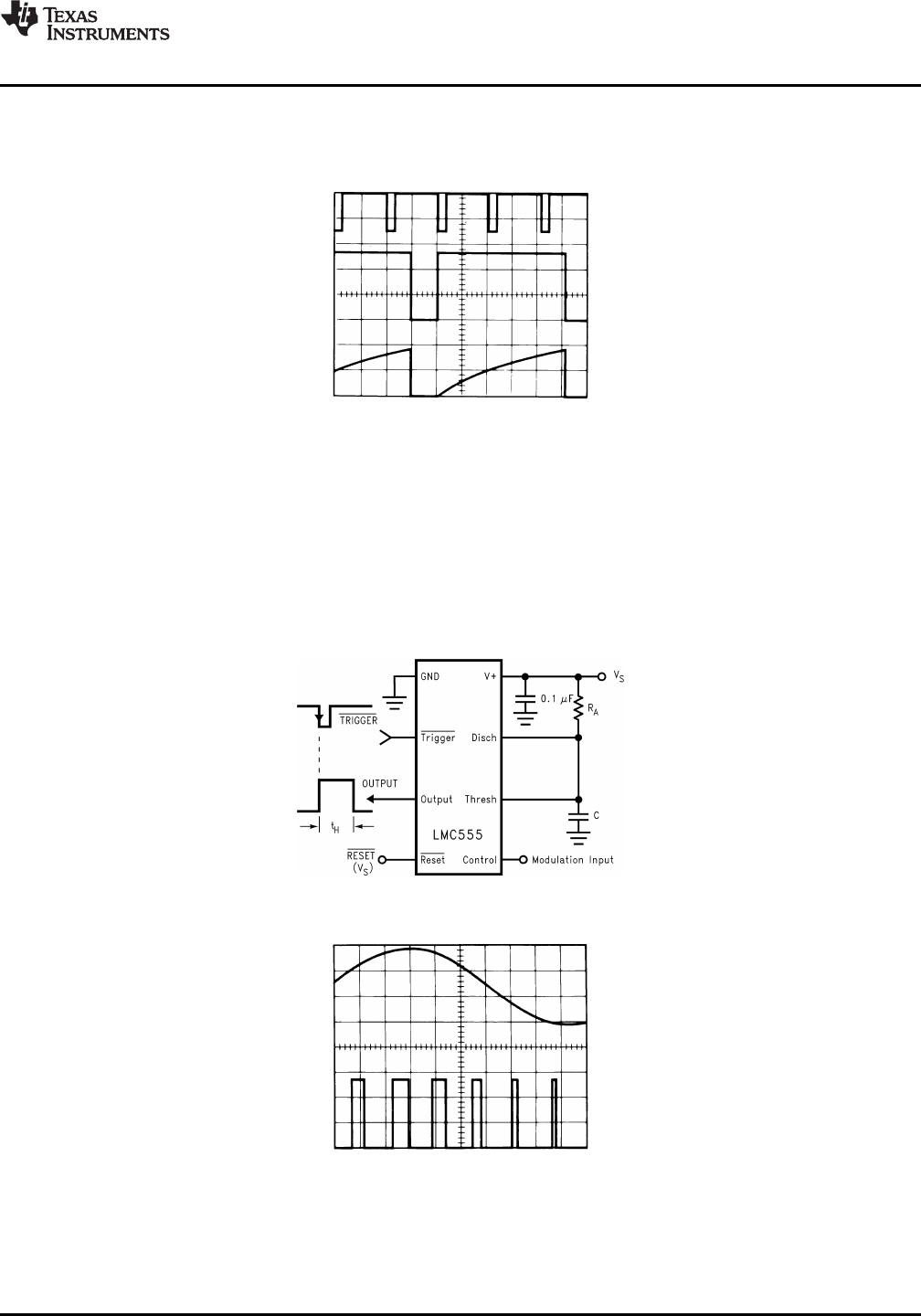
The monostable circuit of Figure 5 can be used as a frequency divider by adjusting the length of the timing cycle.
Figure 11 shows the waveforms generated in a divide by three circuit.
V
CC
= 5V Top Trace: Input 4 V/Div.
TIME = 20 µs/Div. Middle Trace: Output 2 V/Div.
R
A
= 9.1 k Bottom Trace: Capacitor 2 V/Div.
C = 0.01 µF
Figure 11. Frequency Divider Waveforms
PULSE WIDTH MODULATOR
When the timer is connected in the monostable mode and triggered with a continuous pulse train, the output
pulse width can be modulated by a signal applied to the Control Voltage Terminal. Figure 12 shows the circuit,
and in Figure 13 are some waveform examples.
Figure 12. Pulse Width Modulator
V
CC
= 5V Top Trace: Modulation 1 V/Div.
TIME = 0.2 ms/Div. Bottom Trace: Output Voltage 2 V/Div.
R
A
= 9.1 k
C = 0.01 µF
Figure 13. Pulse Width Modulator Waveforms
Copyright © 2000–2013, Texas Instruments Incorporated Submit Documentation Feedback 9
Product Folder Links: LMC555
PREVIOUS1234567NEXT