Closed Dec 25th-26th
800-300-1968
We Stock Hard to Find Parts
My Account
|
My Orders
|
My Cart
Questions?
(800) 300-1968
Register
(current)
My Account
(current)
My Orders
(current)
My Cart
(current)
Categories
(current)
Manufacturers
Request a Quote
Sell Your Excess
Consignment
Quality Assurance
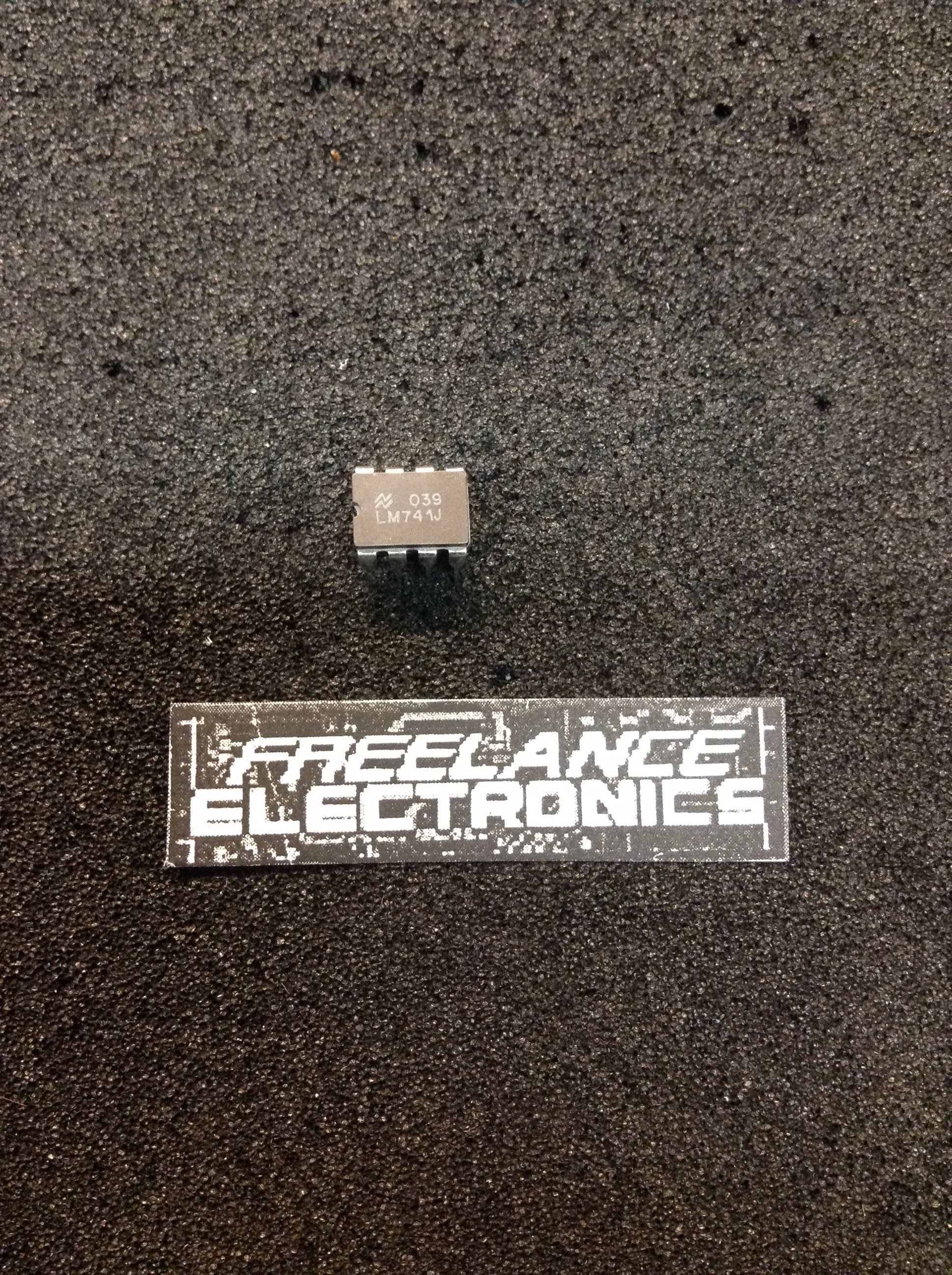
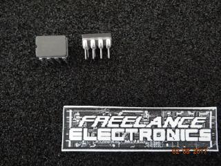
LM741J
Part #
LM741J
Description
OP Amp Single GP ±22V 8-Pin CDip
Category
IC
Availability
Out of Stock
Qty
0
Qty
Price
1 +
$5.67380
Related Items
National Semiconductor Corp
IC
LM741AJ/883B
$11.65231
National Semiconductor Corp
IC
LM741EH
$17.50000
National Semiconductor Corp
IC
LM741F/883B
National Semiconductor Corp
IC
LM741J/883
$7.30425
National Semiconductor Corp
IC
LM741J/883C
$11.31480
National Semiconductor Corp
TRANSISTOR
LM741AH
$9.84723