Closed Dec 25th-26th
800-300-1968
We Stock Hard to Find Parts
My Account
|
My Orders
|
My Cart
Questions?
(800) 300-1968
Register
(current)
My Account
(current)
My Orders
(current)
My Cart
(current)
Categories
(current)
Manufacturers
Request a Quote
Sell Your Excess
Consignment
Quality Assurance
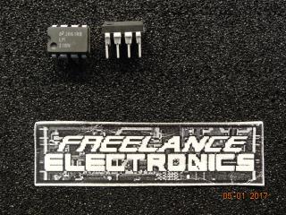
LM318P
Part #
LM318P
Description
HIGH PERFORMANCE OP AMP/LINEAR - Rail/Tube
Category
IC
Availability
Out of Stock
Qty
0
Qty
Price
1 +
$1.71245
Related Items
Advanced Micro Devices
IC
LM318D
$0.81132
National Semiconductor Corp
IC
LM318J-8
$7.43240
National Semiconductor Corp
IC
LM318M
$0.60087
National Semiconductor Corp
IC
LM318N
$0.77175
Fairchild Semiconductor
IC
008-25424
$11.58351
Harris Corporation
IC
01-6945-9