Closed Dec 25th-26th
800-300-1968
We Stock Hard to Find Parts
My Account
|
My Orders
|
My Cart
Questions?
(800) 300-1968
Register
(current)
My Account
(current)
My Orders
(current)
My Cart
(current)
Categories
(current)
Manufacturers
Request a Quote
Sell Your Excess
Consignment
Quality Assurance
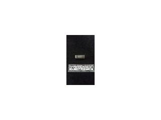
LM1881N
Part #
LM1881N
Description
IC VIDEO SYNC SEPARATOR 8-DIP
Category
IC
Availability
Out of Stock
Qty
0
Qty
Price
1 +
$1.19890
Related Items
National Semiconductor Corp
IC
LM1881M
$1.11380
National Semiconductor Corp
IC
LM1881MX
$0.84379
National Semiconductor Corp
IC
LM1886N
$4.61225
National Semiconductor Corp
IC
LM1889N
$2.43300
Fairchild Semiconductor
IC
008-25424
$11.58351
Harris Corporation
IC
01-6945-9