Freelance Electronics Components Distributor
Closed Dec 25th-26th
800-300-1968
We Stock Hard to Find Parts

LM1086CS-ADJ

Part # LM1086CS-ADJ
Description IC REG LDO ADJ 1.5A DDPAK
Category IC
Availability In Stock
Qty 105
Qty Price
1 - 22 $0.90402
23 - 44 $0.71910
45 - 66 $0.67801
67 - 88 $0.63007
89 + $0.56159
Manufacturer Available Qty
National Semiconductor Corp
  • Shipping Freelance Stock: 15
    Ships Immediately
National Semiconductor Corp
Date Code: 0952
  • Shipping Freelance Stock: 90
    Ships Immediately


Technical Document


DISCLAIMER: The information provided herein is solely for informational purposes. Customers must be aware of the suitability of this product for their application, and consider that variable factors such as Manufacturer, Product Category, Date Codes, Pictures and Descriptions may differ from available inventory.

LM1086
SNVS039H JUNE 2000REVISED MAY 2013
www.ti.com
When the adjustable regulator is used (Figure 21), the best performance is obtained with the positive side of the
resistor R1 tied directly to the output terminal of the regulator rather than near the load. This eliminates line drops
from appearing effectively in series with the reference and degrading regulation. For example, a 5V regulator with
0.05 resistance between the regulator and load will have a load regulation due to line resistance of 0.05 x I
L
.
If R1 (=125) is connected near the load the effective line resistance will be 0.05 (1 + R2/R1) or in this case, it
is 4 times worse. In addition, the ground side of the resistor R2 can be returned near the ground of the load to
provide remote ground sensing and improve load regulation.
Figure 21. Best Load Regulation using Adjustable Output Regulator
PROTECTION DIODES
Under normal operation, the LM1086 regulator does not need any protection diode. With the adjustable device,
the internal resistance between the adjustment and output terminals limits the current. No diode is needed to
divert the current around the regulator even with a capacitor on the adjustment terminal. The adjust pin can take
a transient signal of ±25V with respect to the output voltage without damaging the device.
When an output capacitor is connected to a regulator and the input is shorted, the output capacitor will discharge
into the output of the regulator. The discharge current depends on the value of the capacitor, the output voltage
of the regulator, and rate of decrease of V
IN
. In the LM1086 regulator, the internal diode between the output and
input pins can withstand microsecond surge currents of 10A to 20A. With an extremely large output capacitor
(1000 µf), and with input instantaneously shorted to ground, the regulator could be damaged. In this case, an
external diode is recommended between the output and input pins to protect the regulator, shown in Figure 22.
Figure 22. Regulator with Protection Diode
10 Submit Documentation Feedback Copyright © 2000–2013, Texas Instruments Incorporated
Product Folder Links: LM1086
LM1086
www.ti.com
SNVS039H JUNE 2000REVISED MAY 2013
OVERLOAD RECOVERY
Overload recovery refers to regulator's ability to recover from a short circuited output. A key factor in the recovery
process is the current limiting used to protect the output from drawing too much power. The current limiting circuit
reduces the output current as the input to output differential increases. Refer to short circuit curve in the Typical
Performance Characteristics section.
During normal start-up, the input to output differential is small since the output follows the input. But, if the output
is shorted, then the recovery involves a large input to output differential. Sometimes during this condition the
current limiting circuit is slow in recovering. If the limited current is too low to develop a voltage at the output, the
voltage will stabilize at a lower level. Under these conditions it may be necessary to recycle the power of the
regulator in order to get the smaller differential voltage and thus adequate start up conditions. Refer to Typical
Performance Characteristics section for the short circuit current vs. input differential voltage.
THERMAL CONSIDERATIONS
ICs heats up when in operation, and power consumption is one factor in how hot it gets. The other factor is how
well the heat is dissipated. Heat dissipation is predictable by knowing the thermal resistance between the IC and
ambient (θ
JA
). Thermal resistance has units of temperature per power (C/W). The higher the thermal resistance,
the hotter the IC.
The LM1086 specifies the thermal resistance for each package as junction to case (θ
JC
). In order to get the total
resistance to ambient (θ
JA
), two other thermal resistance must be added, one for case to heat-sink (θ
CH
) and one
for heatsink to ambient (θ
HA
). The junction temperature can be predicted as follows:
T
J
= T
A
+ P
D
(θ
JC
+ θ
CH
+ θ
HA
) = T
A
+ P
D
θ
JA
where
T
J
is junction temperature
T
A
is ambient temperature
P
D
is the power consumption of the device
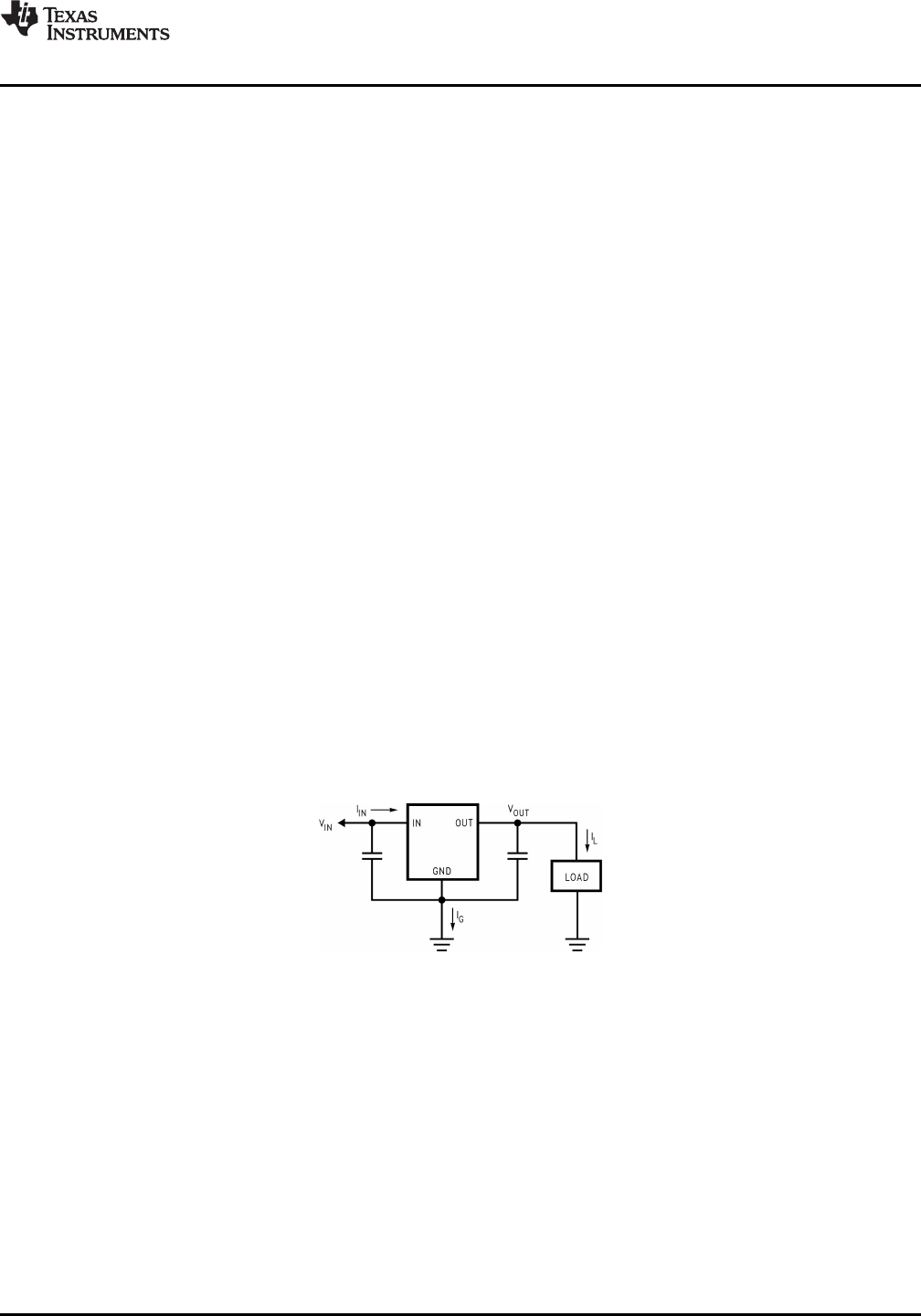
Device power consumption is calculated as follows:
I
IN
= I
L
+ I
G
P
D
= (V
IN
V
OUT
) I
L
+ V
IN
I
G
Figure 23 shows the voltages and currents which are present in the circuit.
Figure 23. Power Dissipation Diagram
Once the device power is determined, the maximum allowable (θ
JA(max)
) is calculated as:
θ
JA (max)
= T
R(max)
/P
D
= T
J(max)
T
A(max)
)/P
D
The LM1086 has different temperature specifications for two different sections of the IC: the control section and
the output section. The Electrical Characteristics table shows the junction to case thermal resistances for each of
these sections, while the maximum junction temperatures (T
J(max)
) for each section is listed in the Absolute
Maximum section of the datasheet. T
J(max)
is 125°C for the control section, while T
J(max)
is 150°C for the output
section.
θ
JA (max)
should be calculated separately for each section as follows:
θ
JA
(max, CONTROL SECTION) = (125°C for T
A(max)
)/P
D
θ
JA
(max, OUTPUT SECTION) = (150°C for T
A(max)
)/P
D
Copyright © 2000–2013, Texas Instruments Incorporated Submit Documentation Feedback 11
Product Folder Links: LM1086
LM1086
SNVS039H JUNE 2000REVISED MAY 2013
www.ti.com
The required heat sink is determined by calculating its required thermal resistance (θ
HA(max)
).
θ
HA(max)
= θ
JA(max)
(θ
JC
+ θ
CH
)
θ
HA (max)
should be calculated twice as follows:
θ
HA (max)
= θ
JA
(max, CONTROL SECTION) - (θ
JC
(CONTROL SECTION) + θ
CH
)
θ
HA (max)
= θ
JA
(max, OUTPUT SECTION) - (θ
JC
(OUTPUT SECTION) + θ
CH
)
If thermal compound is used, θ
CH
can be estimated at 0.2 C/W. If the case is soldered to the heat sink, then a
θ
CH
can be estimated as 0 C/W.
After, θ
HA (max)
is calculated for each section, choose the lower of the two θ
HA (max)
values to determine the
appropriate heat sink.
If PC board copper is going to be used as a heat sink, then Figure 24 can be used to determine the appropriate
area (size) of copper foil required.
Figure 24. Heat sink thermal Resistance vs. Area
Typical Applications
Figure 25. 5V to 3.3V, 1.5A Regulator Figure 26. Adjustable @ 5V
12 Submit Documentation Feedback Copyright © 2000–2013, Texas Instruments Incorporated
Product Folder Links: LM1086
PREVIOUS12345678NEXT