Freelance Electronics Components Distributor
Closed Dec 25th-26th
800-300-1968
We Stock Hard to Find Parts

LM1086CS-ADJ

Part # LM1086CS-ADJ
Description IC REG LDO ADJ 1.5A DDPAK
Category IC
Availability In Stock
Qty 105
Qty Price
1 - 22 $0.90402
23 - 44 $0.71910
45 - 66 $0.67801
67 - 88 $0.63007
89 + $0.56159
Manufacturer Available Qty
National Semiconductor Corp
  • Shipping Freelance Stock: 15
    Ships Immediately
National Semiconductor Corp
Date Code: 0952
  • Shipping Freelance Stock: 90
    Ships Immediately


Technical Document


DISCLAIMER: The information provided herein is solely for informational purposes. Customers must be aware of the suitability of this product for their application, and consider that variable factors such as Manufacturer, Product Category, Date Codes, Pictures and Descriptions may differ from available inventory.

LM1086
www.ti.com
SNVS039H JUNE 2000REVISED MAY 2013
Typical Performance Characteristics (continued)
Ripple Rejection vs. Frequency (LM1086-Adj.) Ripple Rejection vs. Output Current (LM1086-Adj.)
Figure 12. Figure 13.
Ripple Rejection vs. Frequency (LM1086-5) Ripple Rejection vs. Output Current (LM1086-5)
Figure 14. Figure 15.
Line Transient Response Load Transient Response
Figure 16. Figure 17.
Copyright © 2000–2013, Texas Instruments Incorporated Submit Documentation Feedback 7
Product Folder Links: LM1086
LM1086
SNVS039H JUNE 2000REVISED MAY 2013
www.ti.com
APPLICATION NOTE
GENERAL
Figure 18 shows a basic functional diagram for the LM1086-Adj (excluding protection circuitry) . The topology is
basically that of the LM317 except for the pass transistor. Instead of a Darlingtion NPN with its two diode voltage
drop, the LM1086 uses a single NPN. This results in a lower dropout voltage. The structure of the pass transistor
is also known as a quasi LDO. The advantage a quasi LDO over a PNP LDO is its inherently lower quiescent
current. The LM1086 is specified to provide a minimum dropout voltage 1.5V over temperature, at full load.
Figure 18. Basic Functional Diagram for the LM1086, excluding Protection circuitry
OUTPUT VOLTAGE
The LM1086 adjustable version develops at 1.25V reference voltage, (V
REF
), between the output and the adjust
terminal. As shown in figure 2, this voltage is applied across resistor R1 to generate a constant current I1. This
constant current then flows through R2. The resulting voltage drop across R2 adds to the reference voltage to
sets the desired output voltage.
The current I
ADJ
from the adjustment terminal introduces an output error . But since it is small (120uA max), it
becomes negligible when R1 is in the 100 range.
For fixed voltage devices, R1 and R2 are integrated inside the devices.
Figure 19. Basic Adjustable Regulator
STABILITY CONSIDERATION
Stability consideration primarily concern the phase response of the feedback loop. In order for stable operation,
the loop must maintain negative feedback. The LM1086 requires a certain amount series resistance with
capacitive loads. This series resistance introduces a zero within the loop to increase phase margin and thus
increase stability. The equivalent series resistance (ESR) of solid tantalum or aluminum electrolytic capacitors is
used to provide the appropriate zero (approximately 500 kHz).
8 Submit Documentation Feedback Copyright © 2000–2013, Texas Instruments Incorporated
Product Folder Links: LM1086
LM1086
www.ti.com
SNVS039H JUNE 2000REVISED MAY 2013
The Aluminum electrolytic are less expensive than tantalums, but their ESR varies exponentially at cold
temperatures; therefore requiring close examination when choosing the desired transient response over
temperature. Tantalums are a convenient choice because their ESR varies less than 2:1 over temperature.
The recommended load/decoupling capacitance is a 10uF tantalum or a 50uF aluminum. These values will
assure stability for the majority of applications.
The adjustable versions allows an additional capacitor to be used at the ADJ pin to increase ripple rejection. If
this is done the output capacitor should be increased to 22uF for tantalums or to 150uF for aluminum.
Capacitors other than tantalum or aluminum can be used at the adjust pin and the input pin. A 10uF capacitor is
a reasonable value at the input. See RIPPLE REJECTION section regarding the value for the adjust pin
capacitor.
It is desirable to have large output capacitance for applications that entail large changes in load current
(microprocessors for example). The higher the capacitance, the larger the available charge per demand. It is also
desirable to provide low ESR to reduce the change in output voltage:
ΔV = ΔI x ESR
It is common practice to use several tantalum and ceramic capacitors in parallel to reduce this change in the
output voltage by reducing the overall ESR.
Output capacitance can be increased indefinitely to improve transient response and stability.
RIPPLE REJECTION
Ripple rejection is a function of the open loop gain within the feed-back loop (refer to Figure 18 and Figure 19).
The LM1086 exhibits 75dB of ripple rejection (typ.). When adjusted for voltages higher than V
REF
, the ripple
rejection decreases as function of adjustment gain: (1+R1/R2) or V
O
/V
REF
. Therefore a 5V adjustment decreases
ripple rejection by a factor of four (12dB); Output ripple increases as adjustment voltage increases.
However, the adjustable version allows this degradation of ripple rejection to be compensated. The adjust
terminal can be bypassed to ground with a capacitor (C
ADJ
). The impedance of the C
ADJ
should be equal to or
less than R1 at the desired ripple frequency. This bypass capacitor prevents ripple from being amplified as the
output voltage is increased.
1/(2π*f
RIPPLE
*C
ADJ
) R
1
LOAD REGULATION
The LM1086 regulates the voltage that appears between its output and ground pins, or between its output and
adjust pins. In some cases, line resistances can introduce errors to the voltage across the load. To obtain the
best load regulation, a few precautions are needed.
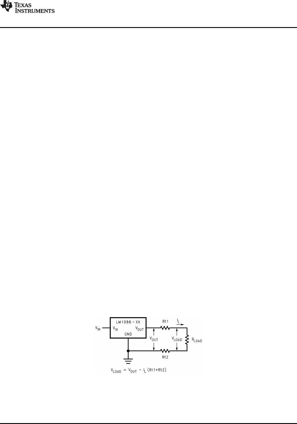
Figure 20 shows a typical application using a fixed output regulator. Rt1 and Rt2 are the line resistances. V
LOAD
is less than the V
OUT
by the sum of the voltage drops along the line resistances. In this case, the load regulation
seen at the R
LOAD
would be degraded from the data sheet specification. To improve this, the load should be tied
directly to the output terminal on the positive side and directly tied to the ground terminal on the negative side.
Figure 20. Typical Application using Fixed Output Regulator
Copyright © 2000–2013, Texas Instruments Incorporated Submit Documentation Feedback 9
Product Folder Links: LM1086
PREVIOUS12345678NEXT