Closed Dec 25th-26th
800-300-1968
We Stock Hard to Find Parts
My Account
|
My Orders
|
My Cart
Questions?
(800) 300-1968
Register
(current)
My Account
(current)
My Orders
(current)
My Cart
(current)
Categories
(current)
Manufacturers
Request a Quote
Sell Your Excess
Consignment
Quality Assurance
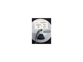
IRF6641PBF
Part #
IRF6641PBF
Description
A 200V Single N-Channel HEXFET Power Mosfet 32Pin MZ
Category
IC
Availability
Out of Stock
Qty
0
Qty
Price
1 +
$6.67934
Related Items
International Rectifier
IC
IRF6614
$3.38112
International Rectifier
IC
IRF6637TR
$3.52231
International Rectifier
RECTIFIER
IRF6612TRPBF
$2.89975
International Rectifier
RECTIFIER
IRF6614TRPBF
$0.82367
International Rectifier
Microcircuit
IRF6616TR1PBF
$3.95100
International Rectifier
CONVERTER
IRF6618PBF
$4.73727