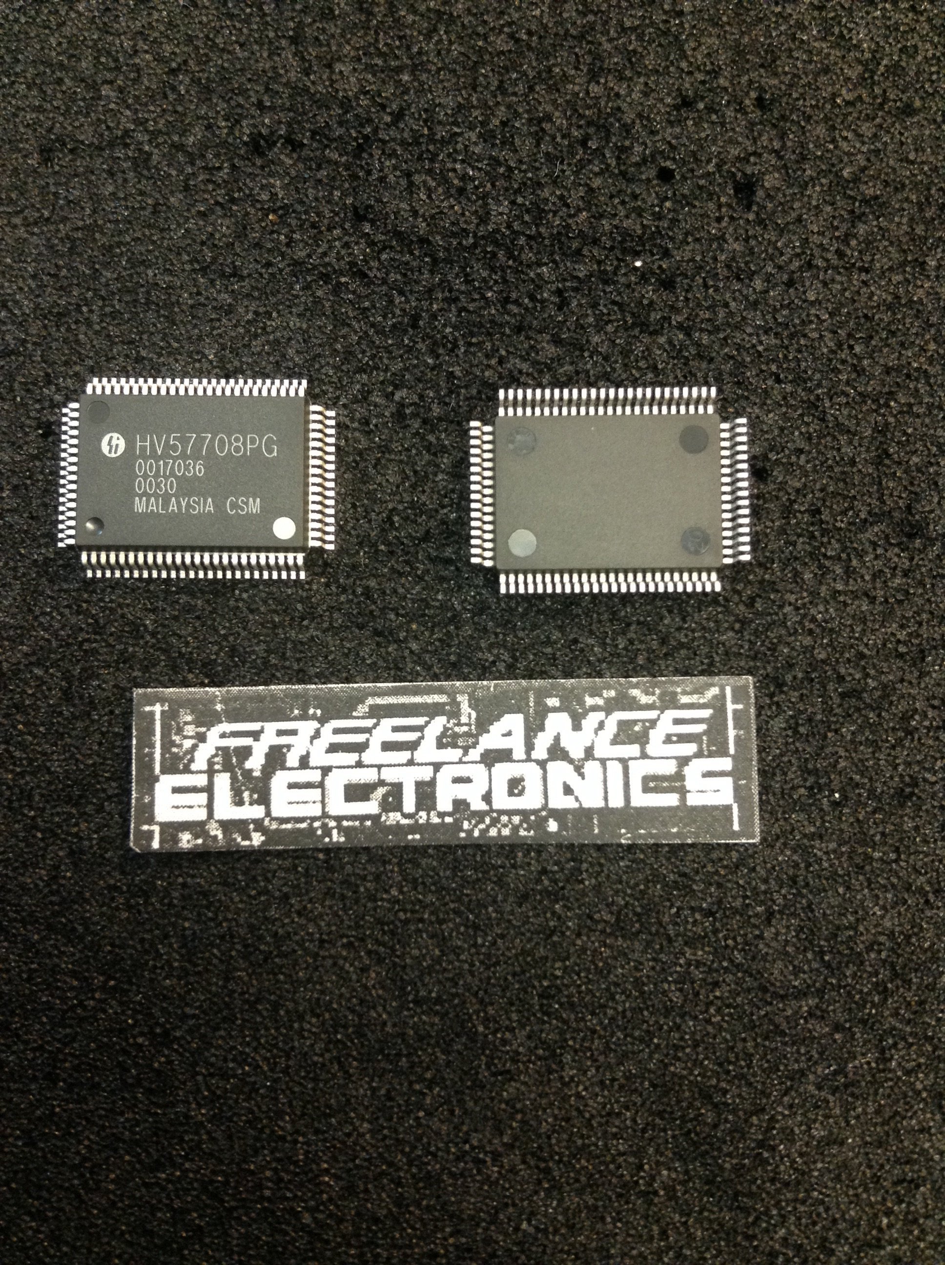
Freelance Electronics Components Distributor
Closed Dec 25th-26th
800-300-1968
We Stock Hard to Find Parts

HV57708PG

Part # HV57708PG
Description Serial to Parallel Logic Converters 80V 32MHz 64Ch P-P
Category IC
Availability In Stock
Qty 55
Qty Price
1 - 11 $20.38869
12 - 23 $16.21828
24 - 34 $15.29152
35 - 46 $14.21030
47 + $12.66570
Manufacturer Available Qty
Supertex
Date Code: 0030
  • Shipping Freelance Stock: 55
    Ships Immediately


Technical Document


DISCLAIMER: The information provided herein is solely for informational purposes. Customers must be aware of the suitability of this product for their application, and consider that variable factors such as Manufacturer, Product Category, Date Codes, Pictures and Descriptions may differ from available inventory.

1
02/96/022
Supertex Inc. does not recommend the use of its products in life support applications and will not knowingly sell its products for use in such applications unless it receives an adequate "products liability
indemnification insurance agreement." Supertex does not assume responsibility for use of devices described and limits its liability to the replacement of devices determined to be defective due to
workmanship. No responsibility is assumed for possible omissions or inaccuracies. Circuitry and specifications are subject to change without notice. For the latest product specifications, refer to the
Supertex website: http://www.supertex.com. For complete liability information on all Supertex products, refer to the most current databook or to the Legal/Disclaimer page on the Supertex website.
HV57708
Device 80 Lead Quad 80 Lead Quad 80 Lead Quad
Ceramic Gullwing Plastic Gullwing Ceramic Gullwing Die
(MIL-STD-883 Processed*) (MIL-STD-883 Processed*)
HV57708 HV57708DG HV57708PG RBHV57708DG HV57708X
* For Hi-Rel process flows, refer to page 5-3 of the Databook.
32 MHz, 64-Channel Serial To Parallel Converter
With Push-Pull Outputs
Ordering Information
Package Options
General Description
The HV577 is a low-voltage serial to high-voltage parallel con-
verter with push-pull outputs. This device has been designed for
use as a driver for electroluminescent displays. It can also be used
in any application requiring multiple output high-voltage current
sourcing and sinking capability such as driving plasma panels,
vacuum fluorescent displays, or large matrix LCD displays.
The device has 4 parallel 16-bit shift registers, permitting data
rates 4X the speed of one ( they are clocked together). There are
also 64 latches and control logic to perform the polarity select and
blanking of the outputs. HVout1 is connected to the first stage of
the first shift register through the polarity and blanking logic. Data
is shifted through the shift registers on the logic low to high
transition of the clock. The DIR pin causes CCW shifting when
connected to GND, and CW shifting when connected to V
DD
. A
data output buffer is provided for cascading devices. This output
reflects the current status of the last bit of the shift register
(HV
OUT
64). Operation of the shift register is not affected by the LE
(latch enable), BL (blanking), or the POL (polarity) inputs. Trans-
fer of data from the shift registers to the latches occurs when the
LE (latch enable) input is high. The data in the latches is stored
when LE is low.
Features
Processed with HVCMOS
®
technology
5V CMOS logic
Output voltages up to 80V
Low power level shifting
32MHz equivalent data rate
Latched data outputs
Forward and reverse shifting options (DIR pin)
Diode to V
PP
allows efficient power recovery
Outputs may be hot switched
Hi-Rel processing available
Absolute Maximum Ratings
Supply voltage, V
DD
1
-0.5V to +7.5V
Output voltage, V
PP
1
-0.5V to +90V
Logic input levels
1
-0.3V to V
DD
+0.3V
Ground current
2
1.5A
Continuous total power dissipation
3
Plastic 1200mW
Ceramic 1900mW
Operating temperature range Plastic -40 to 85°C
Ceramic -55°C to 125°C
Storage temperature range -65°C to +150°C
Lead temperature 1.6mm (1/16 inch) 260°C
from case for 10 seconds
Notes:
1. All voltages are referenced to GND.
2. Limited by the total power dissipated in the package.
3. For operation above 25°C ambient derate linearly to maximum operating
temperature at 20mW/°C for plastic and at 19mW/°C for ceramic.
For detailed circuit and application information, please refer
to application note AN-H3.
2
Symbol Parameter Min Max Units
V
DD
Logic supply voltage 4.5 5.5 V
V
PP
Output voltage 8 80 V
V
IH
High-level input voltage V
DD
-0.5V V
V
IL
Low-level input voltage 0 0.5 V
f
CLK
Clock frequency per register 8 MHz
T
A
Operating free-air temperature Plastic -40 +85
°C
Ceramic -55 +125
Note: Power-up sequence should be the following:
1. Connect ground.
2. Apply V
DD
.
3. Set all inputs (Data, CLK, Enable, etc.) to a known state.
4. Apply V
PP
.
5. The V
PP
should not drop below V
DD
or float during operation.
Power-down sequence should be the reverse of the above.
Electrical Characteristics (over recommended operating conditions unless noted, T
A
=-40°C to +85°C)
DC Characteristics
Symbol Parameter Min Max Units Conditions
I
DD
V
DD
supply current 15 mA V
DD
= V
DD
max
f
CLK
= 8MHz
I
PP
High voltage supply current 100 µA Outputs high
100 µA Outputs low
I
DDQ
Quiescent V
DD
supply current 100 µA All V
IN
= V
DD
V
OH
High-level output HV
OUT
65 V I
O
= -15mA, V
PP
= 80V
Data out V
DD
- 0.5 V I
O
= -100µA
V
OL
Low-level output HV
OUT
7VI
O
= 12mA, V
PP
= 80V
Data out 0.5 V I
O
= 100µA
I
IH
High-level logic input current 1 µAV
IH
= V
DD
I
IL
Low-level logic input current -1 µAV
IL
= 0V
V
OC
High voltage clamp diode 1 V I
OC
= 1mA
Recommended Operating Conditions
AC Characteristics (T
A
= 85°C max. Logic signal inputs and Data inputs have t
r
, t
f
5ns [10% and 90% points])
Symbol Parameter Min Max Units Conditions
f
CLK
Clock frequency 8 MHz Per Register
t
WL
,t
WH
Clock width high or low 62 ns
t
SU
Data set-up time before clock rises 10 ns
t
H
Data hold time after clock rises 15 ns
t
ON
, t
OFF
Time from latch enable to HV
OUT
500 ns C
L
= 15pF
t
DHL
Delay time clock to data high to low 70 ns C
L
= 15pF
t
DLH
Delay time clock to data low to high 70 ns C
L
= 15pF
t
DLE
* Delay time clock to LE low to high 25 ns
t
WLE
Width of LE pulse 25 ns
t
SLE
LE set-up time before clock rises 0 ns
*
t
DLE
is not required but is recommended to produce stable HV outputs and thus minimize power dissipation and current spikes (allows internal SR output to stabilize).
HV57708
3
HV57708
Latch Enable
HV
OUT
w/ S/R LOW
Data Valid50% 50%Data Input
Clock
Data Out
50% 50%
50%
t
SU
t
H
t
WL
t
WH
50%
t
DLH
t
DHL
50%
t
WLE
t
DLE
t
SLE
50%
50%
t
ON
10%
HV
OUT
w/ S/R HIGH
90%
90%
10%
t
OFF
V
IH
V
IL
V
IH
V
IL
V
OH
V
OL
V
OH
V
OL
V
IH
V
OL
V
OH
V
OL
V
OH
V
OL
10%
90%
90%
10% 50%
t
f
t
r
V
DD
Input
GND
V
PP
GND
HV
OUT
Logic Inputs
GND
Data Out
Logic Data Output
High Voltage Outputs
V
DD
Input and Output Equivalent Circuits
Switching Waveforms
12NEXT