Closed Dec 25th-26th
800-300-1968
We Stock Hard to Find Parts
My Account
|
My Orders
|
My Cart
Questions?
(800) 300-1968
Register
(current)
My Account
(current)
My Orders
(current)
My Cart
(current)
Categories
(current)
Manufacturers
Request a Quote
Sell Your Excess
Consignment
Quality Assurance
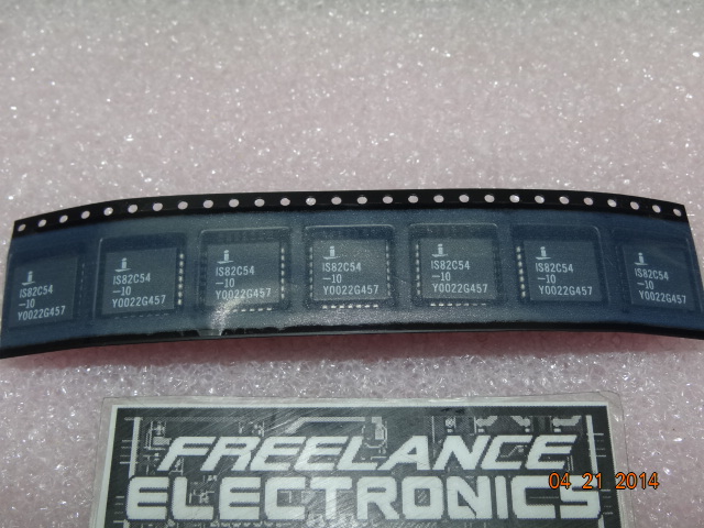
IS82C54-10
Part #
IS82C54-10
Description
PERIPH PRG-CNTR 5V 10MHZ 28PLCC IND
Category
IC
Availability
Out of Stock
Qty
0
Qty
Price
1 +
$2.32553
Related Items
INTERSIL
IC
IS82C52
$225.55071
INTERSIL
IC
IS82C55A
$23.17121
Harris Corporation
IC
IS82C59A-12
$0.68112
Fairchild Semiconductor
IC
008-25424
$11.58351
Harris Corporation
IC
01-6945-9
Motorola Corp
IC
010-143121-0002