Closed Dec 25th-26th
800-300-1968
We Stock Hard to Find Parts
My Account
|
My Orders
|
My Cart
Questions?
(800) 300-1968
Register
(current)
My Account
(current)
My Orders
(current)
My Cart
(current)
Categories
(current)
Manufacturers
Request a Quote
Sell Your Excess
Consignment
Quality Assurance
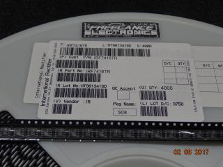
IRF7455
Part #
IRF7455
Description
Trans MOSFET N-CH 30V 15A 8-Pin SOIC - Rail/Tube
Category
IC
Availability
In Stock
Qty
8
Qty
Price
1 +
$1.55243
Manufacturer
Available
Qty
International Rectifier
Date Code: 0405
Freelance Stock:
7
Ships Immediately
International Rectifier
Date Code: 0428
Freelance Stock:
1
Ships Immediately
Add to Cart
Related Items
International Rectifier
IC
IRF7404TRPBF
$0.88543
International Rectifier
IC
IRF7413
$0.30717
International Rectifier
IC
IRF7416
$0.25426
International Rectifier
IC
IRF7416TR
$0.16828
International Rectifier
IC
IRF7420PBF
$0.40180
International Rectifier
IC
IRF7424PBF
$0.34238