Closed Dec 25th-26th
800-300-1968
We Stock Hard to Find Parts
My Account
|
My Orders
|
My Cart
Questions?
(800) 300-1968
Register
(current)
My Account
(current)
My Orders
(current)
My Cart
(current)
Categories
(current)
Manufacturers
Request a Quote
Sell Your Excess
Consignment
Quality Assurance
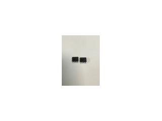
IRF7105TR
Part #
IRF7105TR
Description
DUAL N/P CHANNEL MOSFET, 25V,SOIC, Transistor Polarity:N
Category
IC
Availability
Out of Stock
Qty
0
Qty
Price
1 +
$0.10169
Related Items
International Rectifier
IC
IRF710
$0.33423
International Rectifier
IC
IRF7103
$1.58473
International Rectifier
IC
IRF7103Q
$15.56652
International Rectifier
Microcircuit
IRF7101
$0.78972
International Rectifier
RECTIFIER
IRF711
$0.42007
Fairchild Semiconductor
IC
008-25424
$11.58351