7
®
INA132
APPLICATIONS INFORMATION
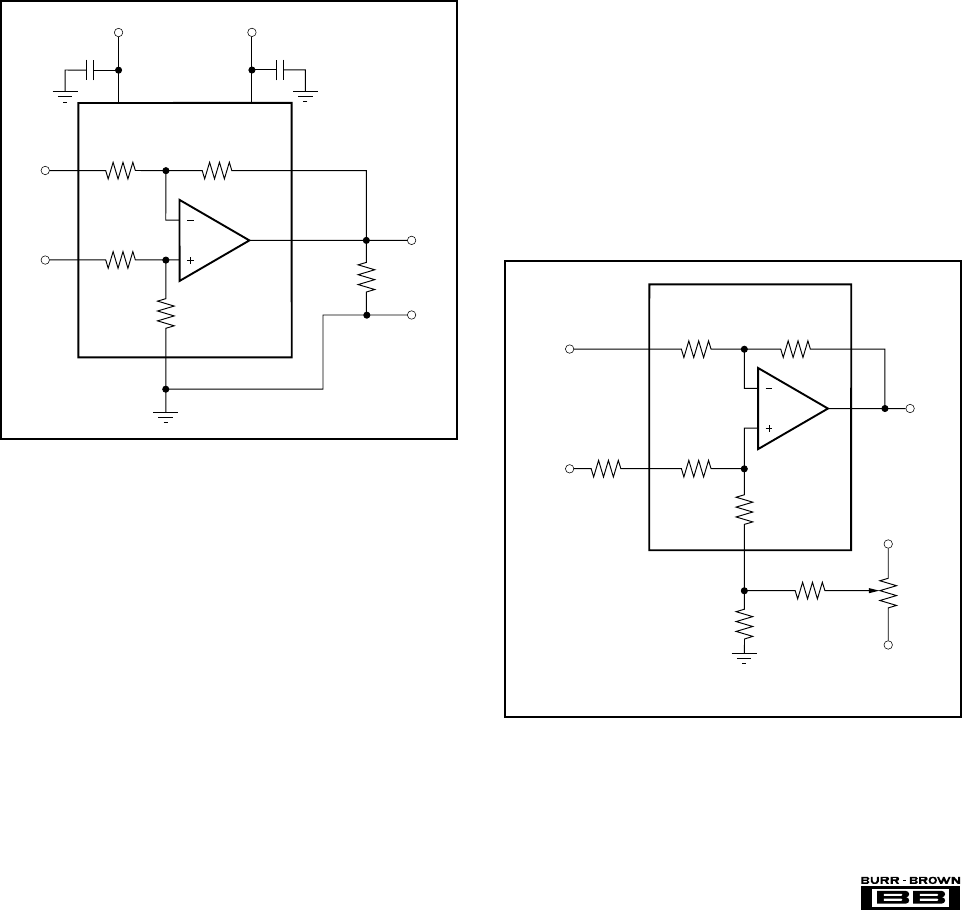
Figure 1 shows the basic connections required for operation
of the INA132. Power supply bypass capacitors should be
connected close to the device pins.
The differential input signal is connected to pins 2 and 3 as
shown. The source impedances connected to the inputs must
be nearly equal to assure good common-mode rejection. An
8Ω mismatch in source impedance will degrade the com-
mon-mode rejection of a typical device to approximately
80dB. Gain accuracy will also be slightly affected. If the
source has a known impedance mismatch, an additional
resistor in series with one input can be used to preserve good
common-mode rejection.
Do not interchange pins 1 and 3 or pins 2 and 5, even though
nominal resistor values are equal. These resistors are laser
trimmed for precise resistor ratios to achieve accurate gain
and highest CMR. Interchanging these pins would not pro-
vide specified performance. As shown in Figure 1, measure-
ments should be sensed at the load.
supply ground). Although input voltages on pins 2 and 3
that are below the negative supply voltage will not damage
the device, operation in this region is not recommended.
Transient conditions at the inverting input terminal below
the negative supply can cause a positive feedback condition
that could lock the INA132’s output to the negative rail.
The INA132 can accurately measure differential signals that
are above the positive power supply. Linear common-mode
range extends to nearly twice the positive power supply
voltage—see typical performance curve, Common-Mode
Range vs Output Voltage.
OFFSET VOLTAGE TRIM
The INA132 is laser trimmed for low offset voltage and drift.
Most applications require no external offset adjustment.
Figure 2 shows an optional circuit for trimming the output
offset voltage. The output is referred to the output reference
terminal (pin 1), which is normally grounded. A voltage
applied to the Ref terminal will be summed with the output
signal. This can be used to null offset voltage. The source
impedance of a signal applied to the Ref terminal should be
less than 8Ω to maintain good common-mode rejection. To
assure low impedance at the Ref terminal, the trim voltage
can be buffered with an op amp, such as the OPA177.
CAPACITIVE LOAD DRIVE CAPABILITY
The INA132 can drive large capacitive loads, even at low
supplies. It is stable with a 10,000pF load. Refer to the
“Small-Signal Step Response” and “Settling Time vs Load
Capacitance” typical performance curves.
FIGURE 1. Basic Power Supply and Signal Connections.
OPERATING VOLTAGE
The INA132 operates from single (+2.7V to +36V) or dual
(±1.35V to ±18V) supplies with excellent performance.
Specifications are production tested with +5V and ±15V
supplies. Most behavior remains unchanged throughout the
full operating voltage range. Parameters which vary signifi-
cantly with operating voltage are shown in the typical
performance curves.
The internal op amp in the INA132 is a single-supply design.
This allows linear operation with the op amp’s common-
mode voltage equal to, or slightly below V– (or single
FIGURE 2. Offset Adjustment.
V
3
5
6
3
V
O
INA132
V
O
= V
3
–
V
2
Offset Adjustment
Range = ±500µV
2
R
3
Ref
R
1
R
2
R
4
V
2
8Ω
R = 237kΩ
8Ω
100kΩ
+15V
–15V
1
NOTE: For ±750µV range, R = 158kΩ.
V
3
5
6
3
INA132
V
OUT
= V
3
–
V
2
2
R
3
Ref
R
1
R
2
R
4
V
2
40kΩ
40kΩ
40kΩ
40kΩ
R
L
1µF
V–
4
1µF
V+
7
1


