Closed Dec 25th-26th
800-300-1968
We Stock Hard to Find Parts
My Account
|
My Orders
|
My Cart
Questions?
(800) 300-1968
Register
(current)
My Account
(current)
My Orders
(current)
My Cart
(current)
Categories
(current)
Manufacturers
Request a Quote
Sell Your Excess
Consignment
Quality Assurance
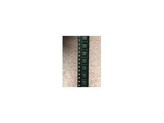
HCPL-5230
Part #
HCPL-5230
Description
OPTOCOUPL LOGIC-OUT THREE STATE DC-IN 2CH 8CDIP - Bulk
Category
IC
Availability
In Stock
Qty
5
Qty
Price
1 - 1
$98.18078
2 - 2
$78.09835
3 - 3
$73.63559
4 +
$68.42903
Manufacturer
Available
Qty
Hewlett-Packard
Date Code: 8644
Freelance Stock:
2
Ships Immediately
Hewlett-Packard
Date Code: 9218
Freelance Stock:
2
Ships Immediately
SGP
Date Code: 0602
Freelance Stock:
1
Ships Immediately
Add to Cart
Related Items
Avago Technologies
IC
HCPL-0211
$2.72424
Hewlett-Packard
IC
HCPL-0453
$1.35848
Avago Technologies
IC
HCPL-0531-500
$17.11702
Hewlett-Packard
IC
HCPL-0611
$1.76295
Agilent technologies Inc
IC
HCPL-063A
$2.43213
Avago Technologies
IC
HCPL-063L
$4.52018