Closed Dec 25th-26th
800-300-1968
We Stock Hard to Find Parts
My Account
|
My Orders
|
My Cart
Questions?
(800) 300-1968
Register
(current)
My Account
(current)
My Orders
(current)
My Cart
(current)
Categories
(current)
Manufacturers
Request a Quote
Sell Your Excess
Consignment
Quality Assurance
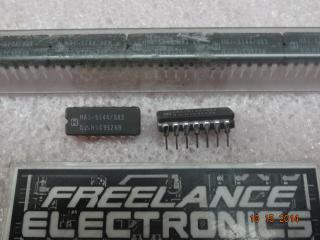
HA1-5104-2
Part #
HA1-5104-2
Description
OP AMP QUAD GP 18V 14CDIP - Rail/Tube
Category
IC
Availability
Out of Stock
Qty
0
Qty
Price
1 +
$21.85400
Related Items
Harris Corporation
IC
HA1-5104-5
$17.98491
Harris Corporation
IC
HA1-5104/883
$57.84416
Harris Corporation
IC
HA1-5104/883C
$25.56935
Harris Corporation
IC
HA1-5114-8
$43.02150
INTERSIL
IC
HA1-5134-5
$24.87970
Harris Corporation
IC
HA1-5144/883
$64.28862