Freelance Electronics Components Distributor
Closed Dec 25th-26th
800-300-1968
We Stock Hard to Find Parts

EPM3032ATC44-10N

Part # EPM3032ATC44-10N
Description CPLD MAX 3000A Family 600 Gates 32 Macro Cells 103.1MHz CM
Category IC
Availability Out of Stock
Qty 0
Qty Price
1 + $2.44490


Technical Document


DISCLAIMER: The information provided herein is solely for informational purposes. Customers must be aware of the suitability of this product for their application, and consider that variable factors such as Manufacturer, Product Category, Date Codes, Pictures and Descriptions may differ from available inventory.

28 Altera Corporation
MAX 3000A Programmable Logic Device Family Data Sheet
Tables 16 through 23 show EPM3032A, EPM3064A, EPM3128A,
EPM3256A, and EPM3512A timing information.
Table 16. EPM3032A External Timing Parameters Note (1)
Symbol Parameter Conditions Speed Grade Unit
–4 –7 –10
Min Max Min Max Min Max
t
PD1
Input to non–
registered output
C1 = 35 pF
(2)
4.5 7.5 10 ns
t
PD2
I/O input to non–
registered output
C1 = 35 pF
(2)
4.5 7.5 10 ns
t
SU
Global clock setup
time
(2) 2.9 4.7 6.3 ns
t
H
Global clock hold time (2) 0.0 0.0 0.0 ns
t
CO1
Global clock to output
delay
C1 = 35 pF 1.0 3.0 1.0 5.0 1.0 6.7 ns
t
CH
Global clock high time 2.0 3.0 4.0 ns
t
CL
Global clock low time 2.0 3.0 4.0 ns
t
ASU
Array clock setup time (2) 1.6 2.5 3.6 ns
t
AH
Array clock hold time (2) 0.3 0.5 0.5 ns
t
ACO1
Array clock to output
delay
C1 = 35 pF
(2)
1.0 4.3 1.0 7.2 1.0 9.4 ns
t
ACH
Array clock high time 2.0 3.0 4.0 ns
t
ACL
Array clock low time 2.0 3.0 4.0 ns
t
CPPW
Minimum pulse width
for clear and preset
(3) 2.0 3.0 4.0 ns
t
CNT
Minimum global clock
period
(2) 4.4 7.2 9.7 ns
f
CNT
Maximum internal
global clock frequency
(2), (4) 227.3 138.9 103.1 MHz
t
ACNT
Minimum array clock
period
(2) 4.4 7.2 9.7 ns
f
ACNT
Maximum internal
array clock frequency
(2), (4) 227.3 138.9 103.1 MHz
Altera Corporation 29
MAX 3000A Programmable Logic Device Family Data Sheet
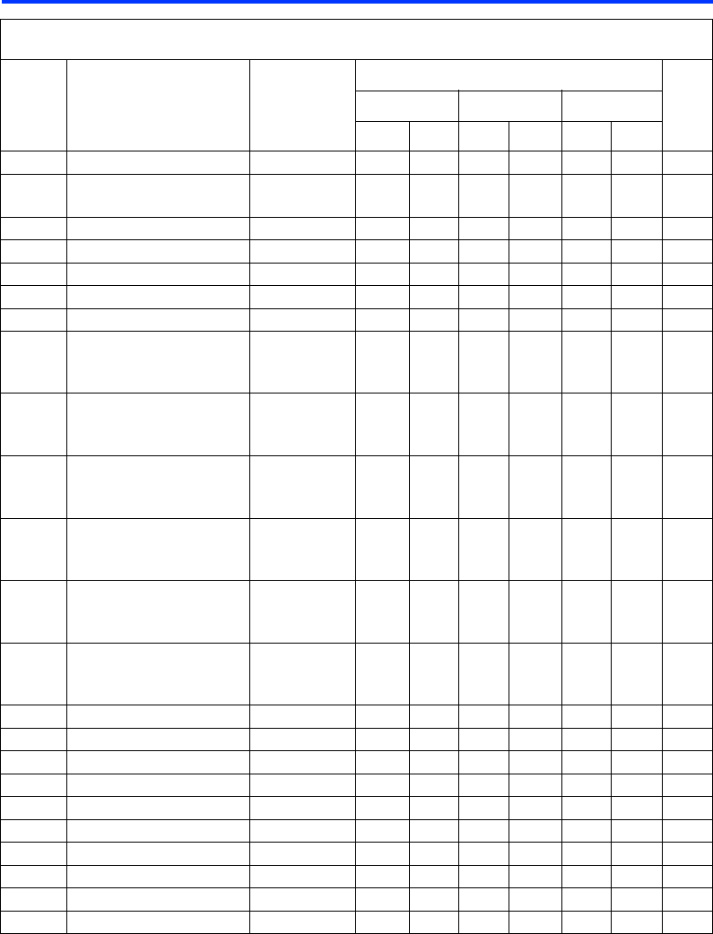
Table 17. EPM3032A Internal Timing Parameters (Part 1 of 2) Note (1)
Symbol Parameter Conditions Speed Grade Unit
–4 –7 –10
Min Max Min Max Min Max
t
IN
Input pad and buffer delay 0.7 1.2 1.5 ns
t
IO
I/O input pad and buffer
delay
0.7 1.2 1.5 ns
t
SEXP
Shared expander delay 1.9 3.1 4.0 ns
t
PEXP
Parallel expander delay 0.5 0.8 1.0 ns
t
LAD
Logic array delay 1.5 2.5 3.3 ns
t
LAC
Logic control array delay 0.6 1.0 1.2 ns
t
IOE
Internal output enable delay 0.0 0.0 0.0 ns
t
OD1
Output buffer and pad
delay, slow slew rate = off
V
CCIO
= 3.3 V
C1 = 35 pF 0.8 1.3 1.8 ns
t
OD2
Output buffer and pad
delay, slow slew rate = off
V
CCIO
= 2.5 V
C1 = 35 pF 1.3 1.8 2.3 ns
t
OD3
Output buffer and pad
delay, slow slew rate = on
V
CCIO
= 2.5 V or 3.3 V
C1 = 35 pF 5.8 6.3 6.8 ns
t
ZX1
Output buffer enable delay,
slow slew rate = off
V
CCIO
= 3.3 V
C1 = 35 pF 4.0 4.0 5.0 ns
t
ZX2
Output buffer enable delay,
slow slew rate = off
V
CCIO
= 2.5 V
C1 = 35 pF 4.5 4.5 5.5 ns
t
ZX3
Output buffer enable delay,
slow slew rate = on
V
CCIO
= 2.5 V or 3.3 V
C1 = 35 pF 9.0 9.0 10.0 ns
t
XZ
Output buffer disable delay C1 = 5 pF 4.0 4.0 5.0 ns
t
SU
Register setup time 1.3 2.0 2.8 ns
t
H
Register hold time 0.6 1.0 1.3 ns
t
RD
Register delay 0.7 1.2 1.5 ns
t
COMB
Combinatorial delay 0.6 1.0 1.3 ns
t
IC
Array clock delay 1.2 2.0 2.5 ns
t
EN
Register enable time 0.6 1.0 1.2 ns
t
GLOB
Global control delay 0.8 1.3 1.9 ns
t
PRE
Register preset time 1.2 1.9 2.6 ns
t
CLR
Register clear time 1.2 1.9 2.6 ns
30 Altera Corporation
MAX 3000A Programmable Logic Device Family Data Sheet
t
PIA
PIA delay (2) 0.9 1.5 2.1 ns
t
LPA
Low–power adder (5) 2.5 4.0 5.0 ns
Table 18. EPM3064A External Timing Parameters Note (1)
Symbol Parameter Conditions Speed Grade Unit
–4 –7 –10
Min Max Min Max Min Max
t
PD1
Input to non–registered
output
C1 = 35 pF (2) 4.5 7.5 10.0 ns
t
PD2
I/O input to non–registered
output
C1 = 35 pF (2) 4.5 7.5 10.0 ns
t
SU
Global clock setup time (2) 2.8 4.7 6.2 ns
t
H
Global clock hold time (2) 0.0 0.0 0.0 ns
t
CO1
Global clock to output delay C1 = 35 pF 1.0 3.1 1.0 5.1 1.0 7.0 ns
t
CH
Global clock high time 2.0 3.0 4.0 ns
t
CL
Global clock low time 2.0 3.0 4.0 ns
t
ASU
Array clock setup time (2) 1.6 2.6 3.6 ns
t
AH
Array clock hold time (2) 0.3 0.4 0.6 ns
t
ACO1
Array clock to output delay C1 = 35 pF (2) 1.04.31.07.21.09.6 ns
t
ACH
Array clock high time 2.0 3.0 4.0 ns
t
ACL
Array clock low time 2.0 3.0 4.0 ns
t
CPPW
Minimum pulse width for
clear and preset
(3) 2.0 3.0 4.0 ns
t
CNT
Minimum global clock
period
(2) 4.5 7.4 10.0 ns
f
CNT
Maximum internal global
clock frequency
(2), (4) 222.2 135.1 100.0 MHz
t
ACNT
Minimum array clock period (2) 4.5 7.4 10.0 ns
f
ACNT
Maximum internal array
clock frequency
(2), (4) 222.2 135.1 100.0 MHz
Table 17. EPM3032A Internal Timing Parameters (Part 2 of 2) Note (1)
Symbol Parameter Conditions Speed Grade Unit
–4 –7 –10
Min Max Min Max Min Max
PREVIOUS345678910111213141516NEXT