Freelance Electronics Components Distributor
Closed Dec 25th-26th
800-300-1968
We Stock Hard to Find Parts

DCP021515U

Part # DCP021515U
Description DC/DC CONV, 2 WATT - Rail/Tube
Category IC
Availability Out of Stock
Qty 0
Qty Price
1 + $6.03755


Technical Document


DISCLAIMER: The information provided herein is solely for informational purposes. Customers must be aware of the suitability of this product for their application, and consider that variable factors such as Manufacturer, Product Category, Date Codes, Pictures and Descriptions may differ from available inventory.

www.ti.com
ADDITIONAL FUNCTIONS
DISABLE/ENABLE
DECOUPLING
Connecting the DCP02 in Parallel
Ripple Reduction
Connecting the DCP02 in Series
DCP 02
+V
OUT
V
SUPPLY
+V
OUT
-V
OUT
-V
OUT
0V
V
S
0V
COM
C requiresalow-ESRceramiccapacitor:5Vto15Vversionis2.2 F;
24Vversionisminimum0.47 F.
m
IN
m
NOTE:(1)
C
IN
(1)
C
1.0 F
OUT
m
C
1.0 F
OUT
m
V
SUPPLY
2xPowerOut
COM
DCP 02
V
OUT
V
S
0V
SYNC
0V
DCP 02
V
OUT
V
S
0V
SYNC
0V
C requiresalow-ESRceramiccapacitor:5Vto15Vversionis2.2 F;
24Vversionisminimum0.47 F.
m
IN
m
NOTE:(1)
C
IN
(1)
C
1.0 F
OUT
m
C
IN
(1)
C
1.0 F
OUT
m
DCP02 Series
SBVS011K MARCH 2000 REVISED FEBRUARY 2008
Connect the positive V
OUT
from one DCP02 to the
The DCP02 can be disabled or enabled by driving the negative V
OUT
(0V) of another (see Figure 7 ). If the
SYNC pin using an open drain CMOS gate. If the SYNC pins are tied together, the self-synchronization
SYNC pin is pulled low, the DCP02 will be disabled. feature of the DCP02 prevents beat frequencies on
The disable time depends upon the external loading; the voltage rails. The SYNC feature of the DCP02
the internal disable function is implemented in 2 µ s. allows easy series connection without external
Removal of the pull down causes the DCP02 to be filtering, thus minimizing cost.
enabled.
The outputs on the dual-output DCP02 versions can
Capacitive loading on the SYNC pin should be also be connected in series to provide two times the
minimized in order to prevent a reduction in the magnitude of V
OUT
, as shown in Figure 8 . For
oscillator frequency. example, a dual 15V DCP022415D could be
connected to provide a 30V rail.
If the output power from one DCP02 is not sufficient,
it is possible to parallel the outputs of multiple
The high switching frequency of 400kHz allows
DCP02s, as shown in Figure 9 . Again, the SYNC
simple filtering. To reduce ripple, it is recommended
feature allows easy synchronization to prevent
that a 1 µ F capacitor be used on V
OUT
. Dual outputs
power-rail beat frequencies at no additional filtering
should both be decoupled to pin 5. A 2.2 µ F capacitor
cost.
on the input is also recommended.
Multiple DCP02 isolated 2W DC/DC converters can
be connected in series to provide nonstandard
voltage rails. This configuration is possible by using
the floating outputs provided by the galvanic isolation
of the DCP02.
Figure 8. Connecting Dual Outputs in Series
Figure 9. Connecting Multiple DCP02s in Parallel
Copyright © 2000 2008, Texas Instruments Incorporated Submit Documentation Feedback 7
Product Folder Link(s): DCP02 Series
www.ti.com
APPLICATION INFORMATION
OPTIMIZING PERFORMANCE
TRANSFORMER DRIVE CIRCUIT
SELF-SYNCHRONIZATION
PCB Design
DCP02 Series
SBVS011K MARCH 2000 REVISED FEBRUARY 2008
The DCP01B , DCV01 , and DCP02 are three families
of miniature DC/DC converters providing an isolated
unregulated voltage output. All are fabricated using a
Optimum performance can only be achieved if the
CMOS/DMOS process with the DCP01B replacing
device is correctly supported. The very nature of a
the familiar DCP01 family that was fabricated from a
switching converter requires power to be instantly
bipolar process. The DCP02 is essentially an
available when it switches on. If the converter has
extension of the DCP01B family, providing a higher
DMOS switching transistors, the fast edges will create
power output with a significantly improved load
a high current demand on the input supply. This
regulation. The DCV01 is tested to a higher isolation
transient load placed on the input is supplied by the
voltage.
external input decoupling capacitor, thus maintaining
the input voltage. Therefore, the input supply does
not see this transient (this is an analogy to
high-speed digital circuits). The positioning of the
Transformer drive transistors have a characteristically
capacitor is critical and must be placed as close as
low value of transistor on resistance (R
DS
); thus, more
possible to the input pins and connected via a
power is transferred to the transformer. The
low-impedance path.
transformer drive circuit is limited by the base current
available to switch on the power transistors driving The optimum performance primarily depends on two
the transformer and the characteristic current gain factors:
(beta), resulting in a slower turn-on time.
1. Connection of the input and output circuits for
Consequently, more power is dissipated within the
minimal loss.
transistor, resulting in a lower overall efficiency,
2. The ability of the decoupling capacitors to
particularly at higher output load currents.
maintain the input and output voltages at a
constant level.
The input synchronizations facility (SYNC
IN
) allows
for easy synchronizing of multiple devices. If two to
The copper losses (resistance and inductance) can
eight devices (maximum) have their respective
be minimized by the use of mutual ground and power
SYNC
IN
pins connected together, then all devices will
planes (tracks) where possible. If that is not possible,
be synchronized.
use wide tracks to reduce the losses. If several
devices are being powered from a common power
Each device has its own onboard oscillator. This
source, a star-connected system for the track must
oscillator is generated by charging a capacitor from a
be deployed; devices must not be connected in
constant current and producing a ramp. When this
series, as this will cascade the resistive losses. The
ramp passes a threshold, an internal switch is
position of the decoupling capacitors is important.
activated that discharges the capacitor to a second
They must be as close to the devices as possible in
threshold before the cycle is repeated.
order to reduce losses. See the PCB Layout section
When several devices are connected together, all the
for more details.
internal capacitors are charged simultaneously.
When one device passes its threshold during the
charge cycle, it starts the discharge cycle. All the
other devices sense this falling voltage and, likewise,
initiate a discharge cycle so that all devices discharge
together. A subsequent charge cycle is only restarted
when the last device has finished its discharge cycle.
8 Submit Documentation Feedback Copyright © 2000 2008, Texas Instruments Incorporated
Product Folder Link(s): DCP02 Series
www.ti.com
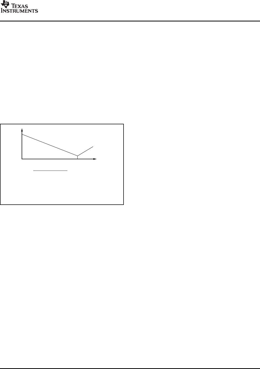
Decoupling Ceramic Capacitors Input Capacitor and the Effects of ESR
0
f
O
Frequency
X
L
Z
Where:
X isthereactanceduetothecapacitance.
C
X isthereactanceduetotheESL.
f istheresonantfrequency.
L
O
Z= (X X )Ö -
C L
2 2
+(ESR)
X
C
DCP02 Series
SBVS011K MARCH 2000 REVISED FEBRUARY 2008
All capacitors have losses because of internal If the input decoupling capacitor is not ceramic with
equivalent series resistance (ESR), and to a lesser <20m ESR, then at the instant the power transistors
degree, equivalent series inductance (ESL). Values switch on, the voltage at the input pins falls
for ESL are not always easy to obtain. However, momentarily. Should the voltage fall below
some manufacturers provide graphs of frequency approximately 4V, the DCP detects an under-voltage
versus capacitor impedance. These graphs typically condition and switches the DCP drive circuits to the
show the capacitor impedance falling as frequency is off state. This detection is carried out as a precaution
increased (as shown in Figure 10 ). As the frequency against a genuine low input voltage condition that
increases, the impedance stops decreasing and could slow down or even stop the internal circuits
begins to rise. The point of minimum impedance from operating correctly. A slow-down or stoppage
indicates the resonant frequency of the capacitor. would result in the drive transistors being turned on
This frequency is where the components of too long, causing saturation of the transformer and
capacitance and inductance reactance are of equal destruction of the device.
magnitude. Beyond this point, the capacitor is not
Following detection of a low input voltage condition,
effective as a capacitor.
the device switches off the internal drive circuits until
the input voltage returns to a safe value. Then the
device tries to restart. If the input capacitor is still
unable to maintain the input voltage, shutdown
recurs. This process is repeated until the capacitor is
charged sufficiently to start the device correctly.
Otherwise, the device will be caught up in a loop.
Normal startup should occur in approximately 1ms
from power being applied to the device. If a
considerably longer startup duration time is
encountered, it is likely that either (or both) the input
supply or the capacitors are not performing
adequately.
For 5V to 15V input devices, a 2.2 µ F low-ESR
ceramic capacitor ensures a good startup
Figure 10. Capacitor Impedance vs Frequency
performance. For the remaining input voltage ranges,
0.47 µ F ceramic capacitors are recommended.
Tantalum capacitors are not recommended, since
At f
O
, X
C
= X
L
; however, there is a 180 ° phase
most do not have low-ESR values and will degrade
difference resulting in cancellation of the imaginary
performance. If tantalum capacitors must be used,
component. The resulting effect is that the impedance
close attention must be paid to both the ESR and
at the resonant point is the real part of the complex
voltage as derated by the vendor.
impedance; namely, the value of the ESR. The
resonant frequency must be well above the 800kHz
Output Ripple Calculation Example
switching frequency of the DCP and DCVs.
DCP020505: Output voltage 5V, Output current 0.4A.
The effect of the ESR is to cause a voltage drop
At full output power, the load resistor is 12.5 . Output
within the capacitor. The value of this voltage drop is
capacitor of 1 µ F, ESR of 0.1 . Capacitor discharge
simply the product of the ESR and the transient load
time 1% of 800kHz (ripple frequency):
current, as shown:
t
DIS
= 0.0125 µ s
V
IN
= V
PK
(ESR × I
TR
) (1)
τ = C × R
LOAD
Where:
τ = 1 × 10
-6
× 12.5 = 12.5 µ s
V
IN
is the voltage at the device input.
V
DIS
= V
O
(1 EXP( t
DIS
/ τ ))
V
PK
is the maximum value of the voltage on the
V
DIS
= 5mV
capacitor during charge.
By contrast, the voltage dropped because of ESR:
I
TR
is the transient load current.
V
ESR
= I
LOAD
× ESR
The other factor that affects the performance is the
V
ESR
= 40mV
value of the capacitance. However, for the input and
Ripple voltage = 45mV
the full wave outputs (single-output voltage devices),
ESR is the dominant factor.
Copyright © 2000 2008, Texas Instruments Incorporated Submit Documentation Feedback 9
Product Folder Link(s): DCP02 Series
PREVIOUS1234567NEXT