FUNCTIONAL DESCRIPTION
OVERVIEW
POWER STAGE
OSCILLATOR AND WATCHDOG
THERMAL SHUTDOWN
CONSTRUCTION
SYNCHRONIZATION
DCP 02
V
OUT1
V
SUPPLY
V
S
0V
V +V
OUT1 OUT2
SYNC
0V
COM
DCP 02
V
OUT2
V
S
0V
SYNC
0V
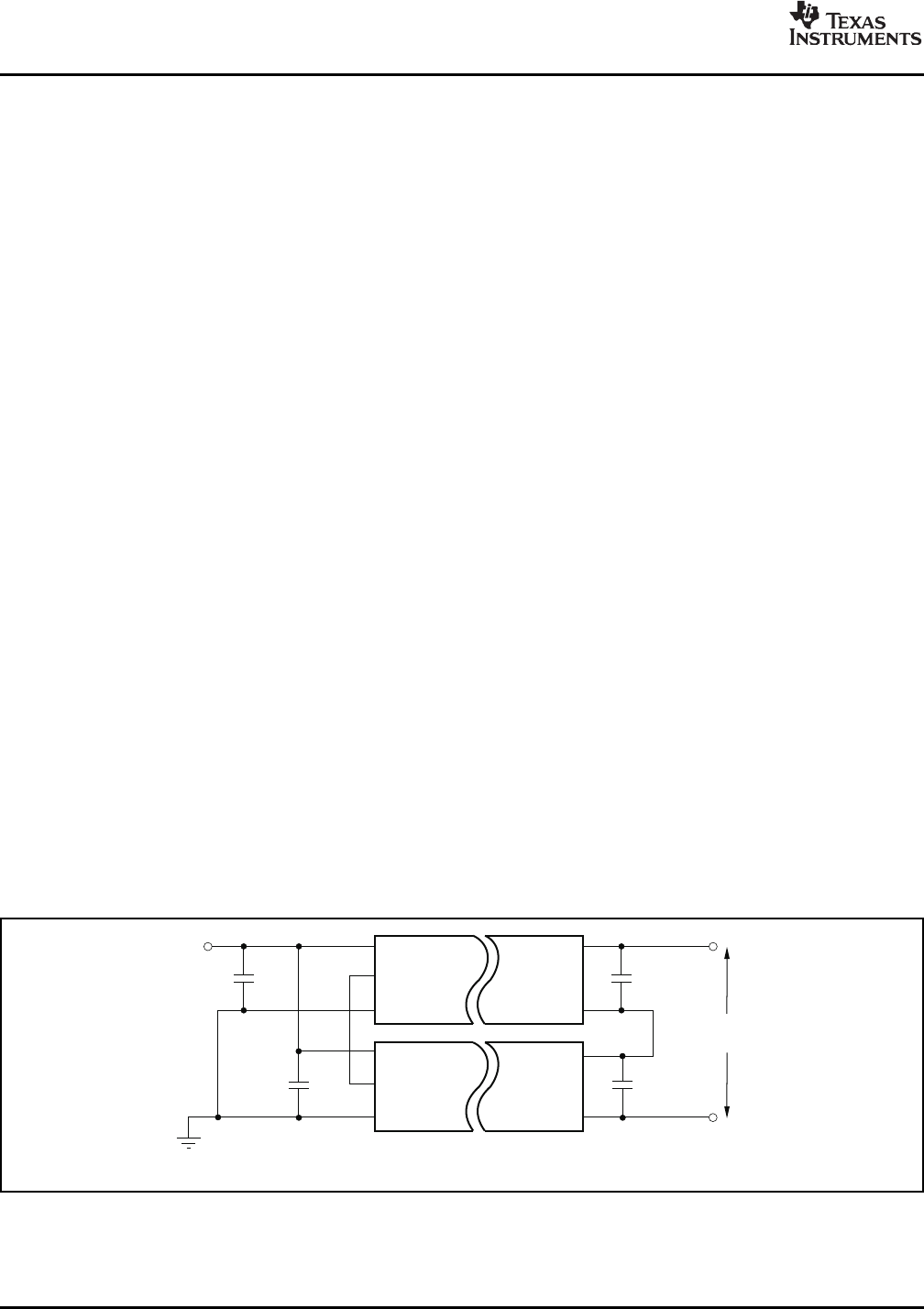
C requiresalow-ESRceramiccapacitor:5Vto15Vversionis2.2 F;
24Vversionisminimum0.47 F.
m
IN
m
NOTE:(1)
C
IN
(1)
C
OUT
1.0 Fm
C
IN
(1)
C
OUT
1.0 Fm
DCP02 Series
SBVS011K – MARCH 2000 – REVISED FEBRUARY 2008
This interference occurs because of the small
variations in switching frequencies between the
The DCP02 offers up to 2W of unregulated output
DC/DC converters.
power from a 5V, 12V, 15V, or 24V input source with
a typical efficiency of up to 89%. This efficiency is The DCP02 overcomes this interference by allowing
achieved through highly integrated packaging devices to be synchronized to one another. Up to
technology and the implementation of a custom eight devices can be synchronized by connecting the
power stage and control IC. The circuit design uses SYNC pins together, taking care to minimize the
an advanced BiCMOS/DMOS process. capacitance of tracking. Stray capacitance (> 10pF)
has the effect of reducing the switching frequency, or
even stopping the oscillator circuit. It is also
recommended that power and ground lines be
The DCP02 uses a push-pull, center-tapped topology
star-connected.
switching at 400kHz (divide-by-2 from an 800kHz
It should be noted that if synchronized devices are
oscillator).
used at start up, all devices will draw maximum
current simultaneously. This configuration can cause
the input voltage to dip; if it dips below the minimum
The onboard 800kHz oscillator generates the
input voltage (4.5V), the devices may not start up. A
switching frequency via a divide-by-2 circuit. The
2.2 µ F capacitor should be connected close to the
oscillator can be synchronized to other DCP02
input pins.
circuits or an external source, and is used to minimize
If more than eight devices are to be synchronized, it
system noise.
is recommended that the SYNC pins be driven by an
A watchdog circuit checks the operation of the
external device. Details are contained in Application
oscillator circuit. The oscillator can be stopped by
Report SBAA035, External Synchronization of the
pulling the SYNC pin low. The output pins will be
DCP01/02 Series of DC/DC Converters , available for
tri-stated, which occurs in 2 µ s.
download from www.ti.com .
The DCP02 is protected by a thermal-shutdown
The basic construction of the DCP02 is the same as
circuit. If the on-chip temperature exceeds +150 ° C,
standard ICs; there is no substrate within the molded
the device will shut down. Once the temperature falls
package. The DCP02 is constructed using an IC,
below +150 ° C, normal operation resumes.
rectifier diodes, and a wound magnetic toroid on a
leadframe. Since there is no solder within the
package, the DCP02 does not require any special
printed circuit board (PCB) assembly processing. This
In the event that more than one DC/DC converter is
architecture results in an isolated DC/DC converter
needed onboard, beat frequencies and other
with inherently high reliability.
electrical interference can be generated.
Figure 7. Connecting the DCP02 in Series
6 Submit Documentation Feedback Copyright © 2000 – 2008, Texas Instruments Incorporated
Product Folder Link(s): DCP02 Series