DS2176
3 of 15
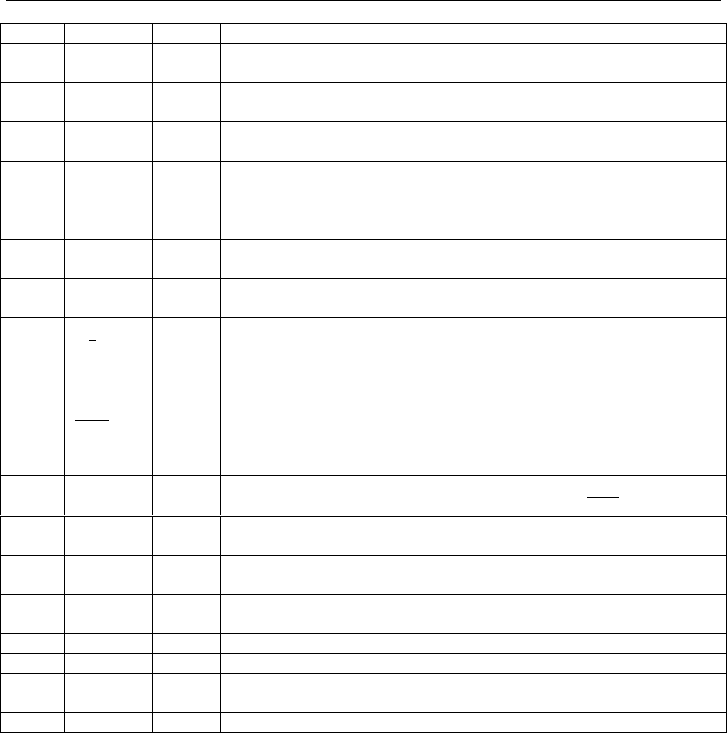
PIN DESCRIPTION Table 1
PIN SYMBOL TYPE DESCRIPTION
1
SIGN
I Signaling Inhibit. When low, ABCD signaling updates are disabled for
a period determined by SM0 and SM1, or until returned high.
2 RMSYNC I Receive Multifram Sync. Must be pulsed high at multiframe
boundaries to establish frame and multiframe alignment.
3 RCLK I Receive Clock. Primary 1.544 MHz clock.
4 RSER I Receive Serial Data. Sampled on Falling edge of RCLK.
5
6
7
8
A
B
C
D
O
Robbed-Bit Signaling Outputs.
9 SCHCLK O System Channel Clock. Transitions high on channel boundaries; useful
for serial to parallel conversion of channel data.
10
11
SM0
SM1
I Signaling Modes 0 and 1. Select signaling supervision technique.
12 V
SS
– Signal Ground. 0.0 volts.
13
S/
I Serial/Parallel Select. Tie to V
SS
for parallel backplane applications, to
V
DD
for serial.
14 FMS I Frame Mode Select. Tie to V
SS
to select 193S(D4) framing to V
DD
for
193E (extended).
15
ALN
I Align. Recenters buffer on next system side frame boundary when
forced low.
16 SFSYNC I System Frame Sync. Rising edge establishes start of frame.
17 SIGFRZ O Signaling Freeze. When high, indicates signaling updates have been
disabled internally via a slip or externally by forcing SIGH low.
18 SMSYNC O System Multiframe Sync. Slip-compensated multiframe output;
indicates when signaling updates are made.
19 SBIT8 O System Bit 8. High during the LSB time of each channel. Used to
reinsert extracted signaling into outgoing data stream.
20
SLIP
O Frame Slip. Active low, open collector output. Held low for 65
SYSCLK cycles when a slip occurs.
21 SSER O System Serial Out. Updated on rising edge of SYSCLK.
22 SYSCLK I System Clock. 1.544 or 2.048 MHz data clock.
23 SCLKSEL I System Clock Select. Tie to V
SS
for 1.544 MHz applications, to V
DD
for
2.048 MHz.
24 V
DD
– Positive Supply. 5.0 volts.


