Closed Dec 25th-26th
800-300-1968
We Stock Hard to Find Parts
My Account
|
My Orders
|
My Cart
Questions?
(800) 300-1968
Register
(current)
My Account
(current)
My Orders
(current)
My Cart
(current)
Categories
(current)
Manufacturers
Request a Quote
Sell Your Excess
Consignment
Quality Assurance
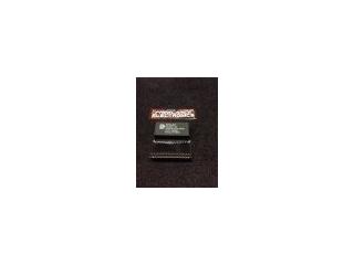
DS1230Y-120
Part #
DS1230Y-120
Description
IC NVSRAM 256KBIT 120NS 28EDIP
Category
IC
Availability
Out of Stock
Qty
0
Qty
Price
1 +
$25.01000
Related Items
DALLAS SEMICONDUCTOR
IC
DS1230Y-85
$31.82915
DALLAS SEMICONDUCTOR
IC
DS1231-20
$4.16526
Military Spec
IC
DS1231-35
$3.20615
DALLAS SEMICONDUCTOR
IC
DS1231S-20
$4.03253
DALLAS SEMICONDUCTOR
IC
DS1231S-20N
$34.44697
DALLAS SEMICONDUCTOR
IC
DS1232-LP
$1.29065