Closed Dec 25th-26th
800-300-1968
We Stock Hard to Find Parts
My Account
|
My Orders
|
My Cart
Questions?
(800) 300-1968
Register
(current)
My Account
(current)
My Orders
(current)
My Cart
(current)
Categories
(current)
Manufacturers
Request a Quote
Sell Your Excess
Consignment
Quality Assurance
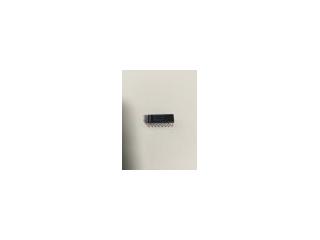
DM74LS175N
Part #
DM74LS175N
Description
Flip Flops Qd D-Type Flip-Flop
Category
IC
Availability
In Stock
Qty
19
Qty
Price
1 +
$0.19546
Manufacturer
Available
Qty
National Semiconductor Corp
Date Code: 9012
Freelance Stock:
19
Ships Immediately
Add to Cart
Related Items
National Semiconductor Corp
IC
DM74L20N
$3.98589
National Semiconductor Corp
IC
DM74L75AN
$3.98589
Fairchild Semiconductor
IC
DM74LS00M
$0.15827
National Semiconductor Corp
IC
DM74LS00N
$0.56545
National Semiconductor Corp
IC
DM74LS01N
$2.41407
Fairchild Semiconductor
IC
DM74LS02M
$0.50176