Closed Dec 25th-26th
800-300-1968
We Stock Hard to Find Parts
My Account
|
My Orders
|
My Cart
Questions?
(800) 300-1968
Register
(current)
My Account
(current)
My Orders
(current)
My Cart
(current)
Categories
(current)
Manufacturers
Request a Quote
Sell Your Excess
Consignment
Quality Assurance
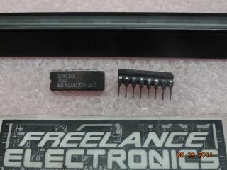
DG441AK
Part #
DG441AK
Description
ANLG SW QUAD SPST 22V/36V16PIN CDIP
Category
IC
Availability
In Stock
Qty
29
Qty
Price
1 - 1
$102.58728
2 - 3
$81.60352
4 - 7
$76.94046
8 - 10
$71.50023
11 +
$63.72846
Manufacturer
Available
Qty
Siliconix
Date Code: 9248
Freelance Stock:
12
Ships Immediately
Siliconix
Date Code: 9230
Freelance Stock:
17
Ships Immediately
Add to Cart
Related Items
INTERSIL
IC
DG441DJ
$1.65045
Siliconix
IC
DG441DY
$0.56495
Siliconix
HYBRID
DG441AK/883
$28.92990
Fairchild Semiconductor
IC
008-25424
$11.58351
Harris Corporation
IC
01-6945-9
Motorola Corp
IC
010-143121-0002