Closed Dec 25th-26th
800-300-1968
We Stock Hard to Find Parts
My Account
|
My Orders
|
My Cart
Questions?
(800) 300-1968
Register
(current)
My Account
(current)
My Orders
(current)
My Cart
(current)
Categories
(current)
Manufacturers
Request a Quote
Sell Your Excess
Consignment
Quality Assurance
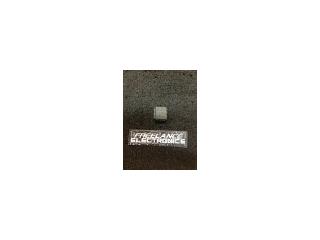
CY7B923-JI
Part #
CY7B923-JI
Description
PHY 1TX-CH 160Mbps/330Mbps 28-Pin PLCC - Rail/Tube
Category
IC
Availability
In Stock
Qty
3
Qty
Price
1 - 2
$37.73421
3 +
$28.58652
Manufacturer
Available
Qty
CYPRESS SEMICONDUCTOR
Date Code: 9920
Freelance Stock:
3
Ships Immediately
Add to Cart
Related Items
CYPRESS SEMICONDUCTOR
IC
CY7B923-LMB
$366.49385
CYPRESS SEMICONDUCTOR
IC
CY7B923-SC
$25.76903
CYPRESS SEMICONDUCTOR
IC
CY7B9294V-BGI
$264.52647
CYPRESS SEMICONDUCTOR
IC
CY7B933-JC
$22.61790
CYPRESS SEMICONDUCTOR
IC
CY7B933-JI
$22.00000
CYPRESS SEMICONDUCTOR
IC
CY7B933-SC
$64.46943