CY54FCT245T, CY74FCT245T
8-BIT TRANSCEIVERS
WITH 3-STATE OUTPUTS
SCCS018B – MAY 1994 – REVISED NOVEMBER 2001
4
POST OFFICE BOX 655303 • DALLAS, TEXAS 75265
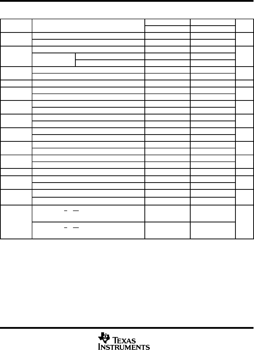
electrical characteristics over recommended operating free-air temperature range (unless
otherwise noted)
CY54FCT245T CY74FCT245T
MIN TYP
†
MAX MIN TYP
†
MAX
V
CC
= 4.5 V, I
IN
= –18 mA –0.7 –1.2
IK
V
CC
= 4.75 V, I
IN
= –18 mA –0.7 –1.2
V
CC
= 4.5 V, I
OH
= –12 mA 2.4 3.3
V
OH
I
OH
= –32 mA 2
V
CC
=
.
I
OH
= –15 mA 2.4 3.3
V
CC
= 4.5 V, I
OL
= 48 mA 0.3 0.55
OL
V
CC
= 4.75 V, I
OL
= 64 mA 0.3 0.55
V
hys
All inputs 0.2 0.2 V
V
CC
= 5.5 V, V
IN
= V
CC
5
I
V
CC
= 5.25 V, V
IN
= V
CC
5
µ
V
CC
= 5.5 V, V
IN
= 2.7 V ±1
IH
V
CC
= 5.25 V, V
IN
= 2.7 V ±1
µ
V
CC
= 5.5 V, V
IN
= 0.5 V ±1
IL
V
CC
= 5.25 V, V
IN
= 0.5 V ±1
µ
V
CC
=
5.5 V, V
OUT
= 2.7 V 10
OZH
V
CC
=
5.25 V, V
OUT
= 2.7 V 10
µ
V
CC
= 5.5 V, V
OUT
= 0.5 V –10
OZL
V
CC
= 5.25 V, V
OUT
= 0.5 V –10
µ
V
CC
= 5.5 V, V
OUT
= 0 V –60 –120 –225
OS
V
CC
= 5.25 V, V
OUT
= 0 V –60 –120 –225
I
off
V
CC
= 0 V, V
OUT
= 4.5 V ±1 ±1 µA
V
CC
= 5.5 V, V
IN
≤ 0.2 V, V
IN
≥ V
CC
– 0.2 V 0.1 0.2
CC
V
CC
= 5.25 V, V
IN
≤ 0.2 V, V
IN
≥ V
CC
– 0.2 V 0.1 0.2
V
CC
= 5.5 V, V
IN
= 3.4 V
§
, f
1
= 0, Outputs open
0.5 2
CC
V
CC
= 5.25 V, V
IN
= 3.4 V
§
, f
1
= 0, Outputs open
0.5 2
V
CC
= 5.5 V, One input switching at 50% duty cycle,
Outputs open, T/R
or OE = GND and
V
IN
≤ 0.2 V or V
IN
≥ V
CC
– 0.2 V
0.06 0.12
mA/
CCD
V
CC
= 5.25 V, One input switching at 50% duty cycle,
Outputs open, T/R
or OE = GND and
V
IN
≤ 0.2 V or V
IN
≥ V
CC
– 0.2 V
0.06 0.12
MHz
†
Typical values are at V
CC
= 5 V, T
A
= 25°C.
‡
Not more than one output should be shorted at a time. Duration of short should not exceed one second. The use of high-speed test apparatus and/or
sample-and-hold techniques are preferable to minimize internal chip heating and more accurately reflect operational values. Otherwise, prolonged
shorting of a high output can raise the chip temperature well above normal and cause invalid readings in other parametric tests. In any sequence
of parameter tests, I
OS
tests should be performed last.
§
Per TTL-driven input (V
IN
= 3.4 V); all other inputs at V
CC
or GND
¶
This parameter is derived for use in total power-supply calculations.