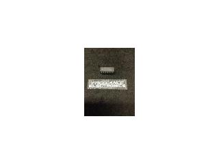
Freelance Electronics Components Distributor
Closed Dec 25th-26th
800-300-1968
We Stock Hard to Find Parts

CD54HCT174F3A

Part # CD54HCT174F3A
Description High Speed CMOS Logic Hex16-CDIP -55 to 125
Category IC
Availability In Stock
Qty 53
Qty Price
1 - 11 $11.84749
12 - 22 $9.42414
23 - 33 $8.88562
34 - 44 $8.25734
45 + $7.35980
Manufacturer Available Qty
Texas Instruments
Date Code: 9930
  • Shipping Freelance Stock: 33
    Ships Immediately
Texas Instruments
Date Code: 9930
  • Shipping Freelance Stock: 20
    Ships Immediately


Technical Document


DISCLAIMER: The information provided herein is solely for informational purposes. Customers must be aware of the suitability of this product for their application, and consider that variable factors such as Manufacturer, Product Category, Date Codes, Pictures and Descriptions may differ from available inventory.

1
Data sheet acquired from Harris Semiconductor
SCHS159C
Features
Buffered Positive Edge Triggered Clock
Asynchronous Common Reset
Fanout (Over Temperature Range)
- Standard Outputs. . . . . . . . . . . . . . . 10 LSTTL Loads
- Bus Driver Outputs . . . . . . . . . . . . . 15 LSTTL Loads
Wide Operating Temperature Range . . . -55
o
C to 125
o
C
Balanced Propagation Delay and Transition Times
Significant Power Reduction Compared to LSTTL
Logic ICs
HC Types
- 2V to 6V Operation
- High Noise Immunity: N
IL
= 30%, N
IH
= 30% of V
CC
at V
CC
= 5V
HCT Types
- 4.5V to 5.5V Operation
- Direct LSTTL Input Logic Compatibility,
V
IL
= 0.8V (Max), V
IH
= 2V (Min)
- CMOS Input Compatibility, I
l
1µA at V
OL
, V
OH
Description
The ’HC174 and ’HCT174 are edge triggered flip-flops which
utilize silicon gate CMOS circuitry to implement D-type flip-
flops. They possess low power and speeds comparable to low
power Schottky TTL circuits. The devices contain six master-
slave flip-flops with a common clock and common reset.
Data on the D input having the specified setup and hold
times is transferred to the Q output on the low to high
transition of the CLOCK input. The
MR input, when low, sets
all outputs to a low state.
Each output can drive ten low power Schottky TTL
equivalent loads. The ’HCT174 is functional as well as, pin
compatible to the ’LS174.
Pinout
CD54HC174, CD54HCT174
(CERDIP)
CD74HC174, CD74HCT174
(PDIP, SOIC)
TOP VIEW
Ordering Information
PART NUMBER
TEMP. RANGE
(
o
C) PACKAGE
CD54HC174F3A -55 to 125 16 Ld CERDIP
CD54HCT174F3A -55 to 125 16 Ld CERDIP
CD74HC174E -55 to 125 16 Ld PDIP
CD74HC174M -55 to 125 16 Ld SOIC
CD74HC174MT -55 to 125 16 Ld SOIC
CD74HC174M96 -55 to 125 16 Ld SOIC
CD74HCT174E -55 to 125 16 Ld PDIP
CD74HCT174M -55 to 125 16 Ld SOIC
CD74HCT174MT -55 to 125 16 Ld SOIC
CD74HCT174M96 -55 to 125 16 Ld SOIC
NOTE: When ordering, use the entire part number. The suffix 96
denotes tape and reel. The suffix T denotes a small-quantity reel of
250.
MR
Q
0
D
0
D
1
Q
1
D
2
GND
V
CC
Q
5
D
5
D
4
Q
4
D
3
Q
3
14
15
16
9
13
12
11
10
1
2
3
4
5
7
6
8
CP
Q
2
August 1997 - Revised October 2003
CAUTION: These devices are sensitive to electrostatic discharge. Users should follow proper IC Handling Procedures.
Copyright
© 2003, Texas Instruments Incorporated
CD54HC174, CD74HC174,
CD54HCT174, CD74HCT174
High-Speed CMOS Logic
Hex D-Type Flip-Flop with Reset
[
/Title
(
CD74
H
C174
,
C
D74
H
CT17
4
)
/
Sub-
j
ect
(
High
S
peed
C
MOS
L
ogic
H
ex D-
T
ype
F
lip-
F
lop
2
Functional Diagram
Logic Diagram
TRUTH TABLE
INPUTS OUTPUT
RESET (MR) CLOCK CP DATA D
n
Q
n
LXXL
H HH
H LL
HLXQ
0
H = High Voltage Level, L = Low Voltage Level, X = Irrelevant, = Transition from Low to
High Level, Q
0
= Level Before the Indicated Steady-State Input Conditions Were Established
CP
D
R
Q
0
Q
1
Q
2
Q
3
Q
4
Q
5
D
0
CP
D
1
D
2
D
3
D
4
D
5
MR
C
L
p
n
C
L
D
n
MR
CP
1
9
3 (4, 6, 11, 13, 14) D
C
L
C
L
C
L
C
L
TO OTHER FIVE F/F
TO OTHER FIVE F/F
R
Q
n
2 (5, 7, 10, 12, 15
)
Q
CP
C
L
p
n
C
L
p
n
C
L
C
L
p
n
816
V
CC
ONE OF SIX F/F
CD54HC174, CD74HC174, CD54HCT174, CD74HCT174
3
Absolute Maximum Ratings Thermal Information
DC Supply Voltage, V
CC
. . . . . . . . . . . . . . . . . . . . . . . . -0.5V to 7V
DC Input Diode Current, I
IK
For V
I
< -0.5V or V
I
> V
CC
+ 0.5V. . . . . . . . . . . . . . . . . . . . . .±20mA
DC Output Diode Current, I
OK
For V
O
< -0.5V or V
O
> V
CC
+ 0.5V . . . . . . . . . . . . . . . . . . . .±20mA
DC Output Source or Sink Current per Output Pin, I
O
For V
O
> -0.5V or V
O
< V
CC
+ 0.5V . . . . . . . . . . . . . . . . . . . .±25mA
DC V
CC
or Ground Current, I
CC or
I
GND
. . . . . . . . . . . . . . . . . .±50mA
Operating Conditions
Temperature Range (T
A
) . . . . . . . . . . . . . . . . . . . . . -55
o
C to 125
o
C
Supply Voltage Range, V
CC
HC Types . . . . . . . . . . . . . . . . . . . . . . . . . . . . . . . . . . . . .2V to 6V
HCT Types . . . . . . . . . . . . . . . . . . . . . . . . . . . . . . . . .4.5V to 5.5V
DC Input or Output Voltage, V
I
, V
O
. . . . . . . . . . . . . . . . . 0V to V
CC
Input Rise and Fall Time
2V . . . . . . . . . . . . . . . . . . . . . . . . . . . . . . . . . . . . . . 1000ns (Max)
4.5V. . . . . . . . . . . . . . . . . . . . . . . . . . . . . . . . . . . . . . 500ns (Max)
6V . . . . . . . . . . . . . . . . . . . . . . . . . . . . . . . . . . . . . . . 400ns (Max)
Thermal Resistance (Typical, Note 1) θ
JA
(
o
C/W)
E (PDIP) Package . . . . . . . . . . . . . . . . . . . . . . . . . . 67
M (SOIC) Package. . . . . . . . . . . . . . . . . . . . . . . . . . 73
Maximum Junction Temperature . . . . . . . . . . . . . . . . . . . . . . . 150
o
C
Maximum Storage Temperature Range . . . . . . . . . .-65
o
C to 150
o
C
Maximum Lead Temperature (Soldering 10s) . . . . . . . . . . . . . 300
o
C
(SOIC - Lead Tips Only)
CAUTION: Stresses above those listed in “Absolute Maximum Ratings” may cause permanent damage to the device. This is a stress only rating and operation
of the device at these or any other conditions above those indicated in the operational sections of this specification is not implied.
NOTE:
1. The package thermal impedance is calculated in accordance with JESD 51-7.
DC Electrical Specifications
PARAMETER SYMBOL
TEST
CONDITIONS
V
CC
(V)
25
o
C -40
o
C TO +85
o
C -55
o
C TO 125
o
C
UNITSV
I
(V) I
O
(mA) MIN TYP MAX MIN MAX MIN MAX
HC TYPES
High Level Input
Voltage
V
IH
- - 2 1.5 - - 1.5 - 1.5 - V
4.5 3.15 - - 3.15 - 3.15 - V
6 4.2 - - 4.2 - 4.2 - V
Low Level Input
Voltage
V
IL
- - 2 - - 0.5 - 0.5 - 0.5 V
4.5 - - 1.35 - 1.35 - 1.35 V
6 - - 1.8 - 1.8 - 1.8 V
High Level Output
Voltage
CMOS Loads
V
OH
V
IH
or
V
IL
-0.02 2 1.9 - - 1.9 - 1.9 - V
-0.02 4.5 4.4 - - 4.4 - 4.4 - V
-0.02 6 5.9 - - 5.9 - 5.9 - V
High Level Output
Voltage
TTL Loads
-4 4.5 3.98 - - 3.84 - 3.7 - V
-5.2 6 5.48 - - 5.34 - 5.2 - V
Low Level Output
Voltage
CMOS Loads
V
OL
V
IH
or
V
IL
0.02 2 - - 0.1 - 0.1 - 0.1 V
0.02 4.5 - - 0.1 - 0.1 - 0.1 V
0.02 6 - - 0.1 - 0.1 - 0.1 V
Low Level Output
Voltage
TTL Loads
4 4.5 - - 0.26 - 0.33 - 0.4 V
5.2 6 - - 0.26 - 0.33 - 0.4 V
Input Leakage
Current
I
I
V
CC
or
GND
-6--±0.1 - ±1-±1 µA
Quiescent Device
Current
I
CC
V
CC
or
GND
0 6 - - 8 - 80 - 160 µA
CD54HC174, CD74HC174, CD54HCT174, CD74HCT174
1234NEXT