Closed Dec 25th-26th
800-300-1968
We Stock Hard to Find Parts
My Account
|
My Orders
|
My Cart
Questions?
(800) 300-1968
Register
(current)
My Account
(current)
My Orders
(current)
My Cart
(current)
Categories
(current)
Manufacturers
Request a Quote
Sell Your Excess
Consignment
Quality Assurance
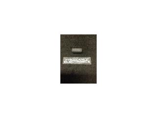
CD54HC75F3A
Part #
CD54HC75F3A
Description
4-BIT LATCH/4-TO-16 LINE DECODER
Category
IC
Availability
In Stock
Qty
8
Qty
Price
1 - 1
$14.05412
2 - 3
$11.17941
4 - 5
$10.54059
6 - 6
$9.79530
7 +
$8.73059
Manufacturer
Available
Qty
RCA
Date Code: 8723
Freelance Stock:
8
Ships Immediately
Add to Cart
Related Items
RCA
IC
CD54HC00F
$1.50230
RCA
IC
CD54HC00F3
RCA
IC
CD54HC00F3A
$7.79537
RCA
IC
CD54HC02F3A
$3.33021
RCA
IC
CD54HC03F3A
$8.06177
RCA
IC
CD54HC04F3A
$6.98714