CC1000
SWRS048A Page 8 of 55
4. Pin Assignment
Pin no. UltraCSP
pin no.
Pin name Pin type Description
1 G3 AVDD Power (A) Power supply (3 V) for analog modules (mixer and IF)
2 F2 AGND Ground (A) Ground connection (0 V) for analog modules (mixer and IF)
3 G2 RF_IN RF Input RF signal input from antenna
4 G1 RF_OUT RF output RF signal output to antenna
5 F1 AVDD Power (A) Power supply (3 V) for analog modules (LNA and PA)
6 E2 AGND Ground (A) Ground connection (0 V) for analog modules (LNA and PA)
7 E1 AGND Ground (A) Ground connection (0 V) for analog modules (PA)
8 D1 AGND Ground (A) Ground connection (0 V) for analog modules (VCO and prescaler)
9 C1 AVDD Power (A) Power supply (3 V) for analog modules (VCO and prescaler)
10 B1 L1 Analog input Connection no 1 for external VCO tank inductor
11 A1 L2 Analog input Connection no 2 for external VCO tank inductor
12 B2 CHP_OUT
(LOCK)
Analog output Charge pump current output
The pin can also be used as PLL Lock indicator. Output is high
when PLL is in lock.
13 C2 R_BIAS Analog output
Connection for external precision bias resistor (82 kΩ, ± 1%)
14 F3 AGND Ground (A) Ground connection (0 V) for analog modules (backplane)
15 A2 AVDD Power (A) Power supply (3 V) for analog modules (general)
16 B3 AGND Ground (A) Ground connection (0 V) for analog modules (general)
17 A3 XOSC_Q2 Analog output Crystal, pin 2
18 A4 XOSC_Q1 Analog input Crystal, pin 1, or external clock input
19 B4 AGND Ground (A) Ground connection (0 V) for analog modules (guard)
20 C3 DGND Ground (D) Ground connection (0 V) for digital modules (substrate)
21 C4 DVDD Power (D) Power supply (3 V) for digital modules
22 D4 DGND Ground (D) Ground connection (0 V) for digital modules
23 E4 DIO Digital
input/output
Data input/output. Data input in transmit mode. Data output in
receive mode
24 F4 DCLK Digital output Data clock for data in both receive and transmit mode
25 G4 PCLK Digital input Programming clock for 3-wire bus
26 D3 PDATA Digital
input/output
Programming data for 3-wire bus. Programming data input for
write operation, programming data output for read operation
27 D2 PALE Digital input Programming address latch enable for 3-wire bus. Internal pull-up.
28 E3 RSSI/IF Analog output The pin can be used as RSSI or 10.7 MHz IF output to optional
external IF and demodulator. If not used, the pin should be left
open (not connected).
A=Analog, D=Digital
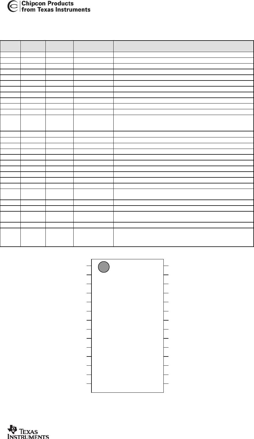
(Top View)
1
14 15
AVDD
AGND
RF_IN
RF_OUT
AVDD
AGND
AGND
AGND
AVDD
L1
L2
R_BIAS
CHP_OUT
AGND
CC1000
2
3
4
6
5
7
8
9
11
12
13
10
28
RSSI/IF
PALE
PDATA
PCLK
DCLK
DIO
DGND
DVDD
DGND
AGND
XOSC_Q1
AGND
XOSC_Q2
AVDD
27
26
25
23
24
22
21
20
18
17
16
19
1
14 15
AVDD
AGND
RF_IN
RF_OUT
AVDD
AGND
AGND
AGND
AVDD
L1
L2
R_BIAS
CHP_OUT
AGND
CC1000
2
3
4
6
5
7
8
9
11
12
13
10
28
RSSI/IF
PALE
PDATA
PCLK
DCLK
DIO
DGND
DVDD
DGND
AGND
XOSC_Q1
AGND
XOSC_Q2
AVDD
RSSI/IF
PALE
PDATA
PCLK
DCLK
DIO
DGND
DVDD
DGND
AGND
XOSC_Q1
AGND
XOSC_Q2
AVDD
27
26
25
23
24
22
21
20
18
17
16
19