1
CA3130, CA3130A
15MHz, BiMOS Operational Amplifier with
MOSFET Input/CMOS Output
CA3130A and CA3130 are op amps that combine the
advantage of both CMOS and bipolar transistors.
Gate-protected P-Channel MOSFET (PMOS) transistors are
used in the input circuit to provide very-high-input
impedance, very-low-input current, and exceptional speed
performance. The use of PMOS transistors in the input stage
results in common-mode input-voltage capability down to
0.5V below the negative-supply terminal, an important
attribute in single-supply applications.
A CMOS transistor-pair, capable of swinging the output
voltage to within 10mV of either supply-voltage terminal (at
very high values of load impedance), is employed as the
output circuit.
The CA3130 Series circuits operate at supply voltages
ranging from 5V to 16V, (±2.5V to ±8V). They can be phase
compensated with a single external capacitor, and have
terminals for adjustment of offset voltage for applications
requiring offset-null capability. Terminal provisions are also
made to permit strobing of the output stage.
The CA3130A offers superior input characteristics over
those of the CA3130.
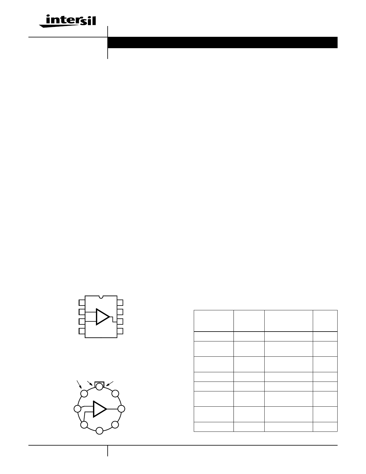
Pinouts
CA3130, CA3130A
(PDIP, SOIC)
TOP VIEW
CA3130, CA3130A
(METAL CAN)
TOP VIEW
Features
• MOSFET Input Stage Provides:
- Very High Z
I
= 1.5 TΩ (1.5 x 10
12
Ω) (Typ)
- Very Low I
I
. . . . . . . . . . . . . 5pA (Typ) at 15V Operation
. . . . . . . . . . . . . . . . . . . . . = 2pA (Typ) at 5V Operation
• Ideal for Single-Supply Applications
• Common-Mode Input-Voltage Range Includes
Negative Supply Rail; Input Terminals can be Swung 0.5V
Below Negative Supply Rail
• CMOS Output Stage Permits Signal Swing to Either (or
both) Supply Rails
Applications
• Ground-Referenced Single Supply Amplifiers
• Fast Sample-Hold Amplifiers
• Long-Duration Timers/Monostables
• High-Input-Impedance Comparators
(Ideal Interface with Digital CMOS)
• High-Input-Impedance Wideband Amplifiers
• Voltage Followers (e.g. Follower for Single-Supply D/A
Converter)
• Voltage Regulators (Permits Control of Output Voltage
Down to 0V)
• Peak Detectors
• Single-Supply Full-Wave Precision Rectifiers
• Photo-Diode Sensor Amplifiers
OFFSET
INV.
NON-INV.
V-
1
2
3
4
8
7
6
5
STROBE
V+
OUTPUT
OFFSET
-
+
NULL
INPUT
INPUT
NULL
TAB
OUTPUT
INV.
V- AND CASE
OFFSET
NON-INV.
V
+
OFFSET
2
4
6
1
3
7
5
8
-
+
STROBE
PHASE
COMPENSATION
NULL
INPUT
INPUT
NULL
Ordering Information
PART NO.
(BRAND)
TEMP.
RANGE
(
o
C) PACKAGE
PKG.
NO.
CA3130AE -55 to 125 8 Ld PDIP E8.3
CA3130AM
(3130A)
-55 to 125 8 Ld SOIC M8.15
CA3130AM96
(3130A)
-55 to 125 8 Ld SOIC
Tape and Reel
M8.15
CA3130AT -55 to 125 8 Pin Metal Can T8.C
CA3130E -55 to 125 8 Ld PDIP E8.3
CA3130M
(3130)
-55 to 125 8 Ld SOIC M8.15
CA3130M96
(3130)
-55 to 125 8 Ld SOIC
Tape and Reel
M8.15
CA3130T -55 to 125
8 Pin Metal Can
T8.C
Data Sheet September 1998 File Number 817.4
CAUTION: These devices are sensitive to electrostatic discharge; follow proper IC Handling Procedures.
1-888-INTERSIL or 321-724-7143
| Copyright © Intersil Corporation 1999


