Freelance Electronics Components Distributor
Closed Dec 25th-26th
800-300-1968
We Stock Hard to Find Parts

BQ2031SN-A5

Part # BQ2031SN-A5
Description IC, LEAD ACID FAST CHARGE16-PIN SOIC
Category IC
Availability In Stock
Qty 56
Qty Price
1 - 11 $6.09344
12 - 23 $4.84705
24 - 35 $4.57008
36 - 47 $4.24694
48 + $3.78532
Manufacturer Available Qty
Texas Instruments
  • Shipping Freelance Stock: 56
    Ships Immediately


Technical Document


DISCLAIMER: The information provided herein is solely for informational purposes. Customers must be aware of the suitability of this product for their application, and consider that variable factors such as Manufacturer, Product Category, Date Codes, Pictures and Descriptions may differ from available inventory.

Pulsed Current Algorithm
In the Pulsed Current algorithm, charging current is
turned off after the initial fast charge termination until
V
CELL
falls to V
FLT
. Full fast charge current (I
MAX
)is
then re-enabled to the battery until V
CELL
rises to V
BLK
.
This cycle repeats indefinitely.
Charge Regulation
The bq2031 controls charging through pulse-width modu-
lation of the MOD output pin, supporting both constant-
current and constant-voltage regulation. Charge current
is monitored by the voltage at the SNS pin, and charge
voltage by voltage at the BAT pin. These voltages are
compared to an internal temperature-compensated refer-
ence, and the MOD output modulated to maintain the de-
sired value.
Voltage at the SNS pin is determined by the value of re
-
sistor R
SNS
, so nominal regulated current is set by:
Equation 8
I
MAX
= 0.250V/R
SNS
The switching frequency of the MOD output is deter
-
mined by an external capacitor (CPWM) between the
pin TPWM and ground, per the following:
Equation 9
F
PWM
= 0.1/C
PWM
where C is in
µ
F and F is in kHz. A typical switching
rate is 100kHz, implying C
PWM
= 0.001
µ
F. MOD pulse
width is modulated between 0 and 80% of the switching
period.
To prevent oscillation in the voltage and current control
loops, frequency compensation networks (C or R-C) are
typically required on the VCOMP and ICOMP pins (respec
-
tively) to add poles and zeros to the loop control equations.
A software program, “CNFG2031,” is available to assist in
configuring these networks for buck type regulators. For
more detail on the control loops in buck topology, see the
application note, “Switch-Mode Power Conversion Using
the bq2031.” For assistance with other power supply topolo-
gies, contact the factory.
10
bq2031
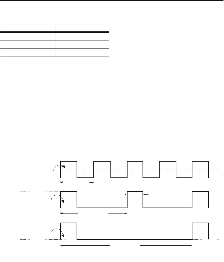
IGSEL T
P
(sec.)
L 0.4
H 0.8
Z 1.6
Table 4. Fixed-Pulse Period by IGSEL
TD203101.eps
I
COND
I
COND
I
COND
0
0
0
IGSEL = L
Ave. Current
IGSEL = H
Ave. Current
IGSEL = Z
Ave. Current
T
P
= 1.6 Sec
T
P
= 0.8 Sec
T
P
= 0.4 Sec
0.2 Sec
Figure 10. Implementation of Fixed-Pulse Maintenance Charge
11
bq2031
Absolute Maximum Ratings
Symbol Parameter Minimum Maximum Unit Notes
V
CC
V
CC
relative to V
SS
-0.3 +7.0 V
V
T
DC voltage applied on any pin ex
-
cluding V
CC
relative to V
SS
-0.3 +7.0 V
T
OPR
Operating ambient temperature -20 +70 °C Commercial
T
STG
Storage temperature -55 +125 °C
T
SOLDER
Soldering temperature - +260 °C 10 s. max.
T
BIAS
Temperature under bias -40 +85 °C
Note: Permanent device damage may occur if Absolute Maximum Ratings are exceeded. Functional opera
-
tion should be limited to the Recommended DC Operating Conditions detailed in this data sheet. Expo
-
sure to conditions beyond the operational limits for extended periods of time may affect device reliability.
DC Thresholds (T
A
= T
OPR
;V
CC
= 5V
±
10%)
Symbol Parameter Rating Unit Tolerance Notes
V
REF
Internal reference voltage 2.20 V 1% T
A
= 25°C
Temperature coefficient -3.9 mV/°C 10%
V
LTF
TS maximum threshold 0.6
*
V
CC
V
±
0.03V Low-temperature fault
V
HTF
TS hysteresis threshold 0.44
*
V
CC
V
±
0.03V High-temperature fault
V
TCO
TS minimum threshold 0.4
*
V
CC
V
±
0.03V Temperature cutoff
V
HCO
High cutoff voltage 0.60
*
V
CC
V
±
0.03V
V
MIN
Under-voltage threshold at BAT 0.34
*
V
CC
V
±
0.03V
V
LCO
Low cutoff voltage 0.8 V
±
0.03V
V
SNS
Current sense at SNS
0.250 V 10% I
MAX
0.05 V 10% I
COND
12
bq2031
Recommended DC Operating Conditions (T
A
= T
OPR)
Symbol Parameter Minimum Typical Maximum Unit Notes
V
CC
Supply voltage 4.5 5.0 5.5 V
V
TEMP
TS voltage potential 0 - V
CC
VV
TS
- V
SNS
V
CELL
Battery voltage potential 0 - V
CC
VV
BAT
- V
SNS
I
CC
Supply current - 2 4 mA Outputs unloaded
I
IZ
DSEL tri-state open detection -2 - 2
µ
A Note 2
IGSEL tri-state open detection -2 2
µ
A
V
IH
Logic input high
V
CC
-1.0 - - V QSEL,TSEL
V
CC
-0.3 - - V DSEL, IGSEL
V
IL
Logic input low
--V
SS
+1.0 V QSEL,TSEL
--V
SS
+0.3 V DSEL, IGSEL
V
OH
LED
1
, LED
2
, LED
3
, output high V
CC
-0.8 - - V I
OH
10mA
MOD output high V
CC
-0.8 - - V I
OH
10mA
V
OL
LED
1
, LED
2
, LED
3
, output low - - V
SS
+0.8V V I
OL
10mA
MOD output low - - V
SS
+0.8V V I
OL
10mA
FLOAT output low - - V
SS
+0.8V V I
OL
5mA, Note 3
COM output low - - V
SS+
0.5 V I
OL
30mA
I
OH
LED
1
, LED
2
, LED
3
, source -10 - - mA V
OH
=V
CC
-0.5V
MOD source -5.0 - - mA V
OH
=V
CC
-0.5V
I
OL
LED
1
, LED
2
, LED
3
, sink 10 - - mA V
OL
= V
SS
+0.5V
MOD sink 5 - - mA V
OL
= V
SS
+0.8V
FLOAT sink 5 - - mA V
OL
= V
SS
+0.8V, Note 3
COM sink 30 - - mA V
OL
= V
SS
+0.5V
I
IL
DSEL logic input low source - - +30
µ
A V = V
SS
to V
SS
+ 0.3V, Note 2
IGSEL logic input low source - - +70
µ
A V = V
SS
to V
SS
+ 0.3V
I
IH
DSEL logic input high source -30 - -
µ
A V = V
CC
- 0.3V to V
CC
IGSEL logic input high source -70 - -
µ
A V = V
CC
- 0.3V to V
CC
I
L
Input leakage - -
±
1
µ
A QSEL, TSEL, Note 2
Notes: 1. All voltages relative to V
SS
except where noted.
2. Conditions during initialization after V
CC
applied.
3. SNS = 0V.
PREVIOUS1234567NEXT