Closed Dec 25th-26th
800-300-1968
We Stock Hard to Find Parts
My Account
|
My Orders
|
My Cart
Questions?
(800) 300-1968
Register
(current)
My Account
(current)
My Orders
(current)
My Cart
(current)
Categories
(current)
Manufacturers
Request a Quote
Sell Your Excess
Consignment
Quality Assurance
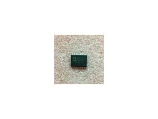
ADUM1100BR
Part #
ADUM1100BR
Description
100 MBD SINGLE CHANNEL DIGITAL ISOLATOR - Rail/Tube
Category
IC
Availability
Out of Stock
Qty
0
Qty
Price
1 +
$1.53657
Related Items
Analog Devices
IC
ADUM1200ARZ
$1.23019
Generic
IC
ADUM1200BR
$4.00227
Analog Devices
IC
ADUM1201BRZ-RL7
$1.62000
Analog Devices
IC
ADUM1400BRW
$1.06382
Analog Devices
IC
ADUM1401BRW
$4.53116
Analog Devices
IC
ADUM1401WSRWZ
$3.15049