Freelance Electronics Components Distributor
Closed Dec 25th-26th
800-300-1968
We Stock Hard to Find Parts

ATMEGA48-20AU

Part # ATMEGA48-20AU
Description MCU 8BIT ATMEGA RISC 4KB FLASH 3.3V/5V 32TQFP - Trays
Category IC
Availability Out of Stock
Qty 0
Qty Price
1 + $1.49230


Technical Document


DISCLAIMER: The information provided herein is solely for informational purposes. Customers must be aware of the suitability of this product for their application, and consider that variable factors such as Manufacturer, Product Category, Date Codes, Pictures and Descriptions may differ from available inventory.

295
2545M–AVR–09/07
ATmega48/88/168
Figure 27-2. Addressing the Flash Which is Organized in Pages
(1)
Note: 1. PCPAGE and PCWORD are listed in Table 27-9 on page 290.
Figure 27-3. Programming the Flash Waveforms
(1)
Note: 1. “XX” is don’t care. The letters refer to the programming description above.
27.7.5 Programming the EEPROM
The EEPROM is organized in pages, see Table 27-10 on page 290. When programming the
EEPROM, the program data is latched into a page buffer. This allows one page of data to be
programmed simultaneously. The programming algorithm for the EEPROM data memory is as
follows (refer to “Programming the Flash” on page 293 for details on Command, Address and
Data loading):
1. A: Load Command “0001 0001”.
2. G: Load Address High Byte (0x00 - 0xFF).
3. B: Load Address Low Byte (0x00 - 0xFF).
4. C: Load Data (0x00 - 0xFF).
PROGRAM MEMORY
WORD ADDRESS
WITHIN A PAGE
PAGE ADDRESS
WITHIN THE FLASH
INSTRUCTION WORD
PAG E
PCWORD[PAGEMSB:0]:
00
01
02
PAGEEND
PAG E
PCWORDPCPAGE
PCMSB
PAGEMSB
PROGRAM
COUNTER
RDY/BSY
WR
OE
ESET +12V
PAGEL
BS2
0x10 ADDR. LOW
ADDR. HIGH
DATA
DATA LOW DATA HIGH
ADDR. LOW DATA LOW DATA HIGH
XA1
XA0
BS1
XTAL1
XX XX
XX
ABCDEBCDEGH
296
2545M–AVR–09/07
ATmega48/88/168
5. E: Latch data (give PAGEL a positive pulse).
K: Repeat 3 through 5 until the entire buffer is filled.
L: Program EEPROM page
1. Set BS1 to “0”.
2. Give WR
a negative pulse. This starts programming of the EEPROM page. RDY/BSY
goes low.
3. Wait until to RDY/BSY
goes high before programming the next page (See Figure 27-4 for
signal waveforms).
Figure 27-4. Programming the EEPROM Waveforms
27.7.6 Reading the Flash
The algorithm for reading the Flash memory is as follows (refer to “Programming the Flash” on
page 293 for details on Command and Address loading):
1. A: Load Command “0000 0010”.
2. G: Load Address High Byte (0x00 - 0xFF).
3. B: Load Address Low Byte (0x00 - 0xFF).
4. Set OE
to “0”, and BS1 to “0”. The Flash word low byte can now be read at DATA.
5. Set BS1 to “1”. The Flash word high byte can now be read at DATA.
6. Set OE
to “1”.
27.7.7 Reading the EEPROM
The algorithm for reading the EEPROM memory is as follows (refer to “Programming the Flash”
on page 293 for details on Command and Address loading):
1. A: Load Command “0000 0011”.
2. G: Load Address High Byte (0x00 - 0xFF).
3. B: Load Address Low Byte (0x00 - 0xFF).
4. Set OE
to “0”, and BS1 to “0”. The EEPROM Data byte can now be read at DATA.
5. Set OE
to “1”.
RDY/BSY
WR
OE
R
ESET +12V
PAGEL
BS2
0x11 ADDR. HIGH
DATA
ADDR. LOW DATA ADDR. LOW DATA XX
XA1
XA0
BS1
XTAL1
XX
AGBCEBC EL
K
297
2545M–AVR–09/07
ATmega48/88/168
27.7.8 Programming the Fuse Low Bits
The algorithm for programming the Fuse Low bits is as follows (refer to “Programming the Flash”
on page 293 for details on Command and Data loading):
1. A: Load Command “0100 0000”.
2. C: Load Data Low Byte. Bit n = “0” programs and bit n = “1” erases the Fuse bit.
3. Give WR
a negative pulse and wait for RDY/BSY to go high.
27.7.9 Programming the Fuse High Bits
The algorithm for programming the Fuse High bits is as follows (refer to “Programming the
Flash” on page 293 for details on Command and Data loading):
1. A: Load Command “0100 0000”.
2. C: Load Data Low Byte. Bit n = “0” programs and bit n = “1” erases the Fuse bit.
3. Set BS1 to “1” and BS2 to “0”. This selects high data byte.
4. Give WR
a negative pulse and wait for RDY/BSY to go high.
5. Set BS1 to “0”. This selects low data byte.
27.7.10 Programming the Extended Fuse Bits
The algorithm for programming the Extended Fuse bits is as follows (refer to “Programming the
Flash” on page 293 for details on Command and Data loading):
1. 1. A: Load Command “0100 0000”.
2. 2. C: Load Data Low Byte. Bit n = “0” programs and bit n = “1” erases the Fuse bit.
3. 3. Set BS1 to “0” and BS2 to “1”. This selects extended data byte.
4. 4. Give WR
a negative pulse and wait for RDY/BSY to go high.
5. 5. Set BS2 to “0”. This selects low data byte.
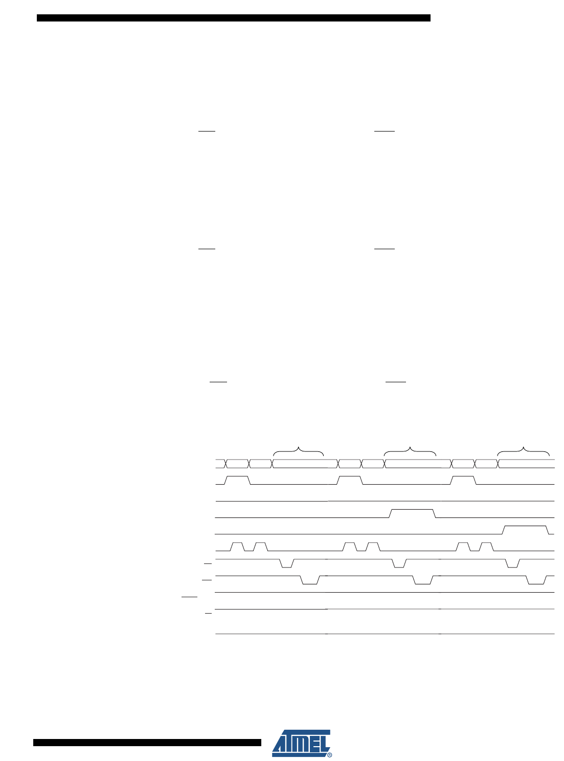
Figure 27-5. Programming the FUSES Waveforms
27.7.11 Programming the Lock Bits
The algorithm for programming the Lock bits is as follows (refer to “Programming the Flash” on
page 293 for details on Command and Data loading):
RDY/BSY
WR
OE
RESET +12V
PAGEL
0x40
DATA
DATA XX
XA1
XA0
BS1
XTAL1
AC
0x40 DATA XX
AC
Write Fuse Low byte Write Fuse high byte
0x40 DATA XX
AC
Write Extended Fuse byte
BS2
PREVIOUS9293949596979899100101102103104105NEXT