Freelance Electronics Components Distributor
Closed Dec 25th-26th
800-300-1968
We Stock Hard to Find Parts

ATMEGA48-20AU

Part # ATMEGA48-20AU
Description MCU 8BIT ATMEGA RISC 4KB FLASH 3.3V/5V 32TQFP - Trays
Category IC
Availability Out of Stock
Qty 0
Qty Price
1 + $1.49230


Technical Document


DISCLAIMER: The information provided herein is solely for informational purposes. Customers must be aware of the suitability of this product for their application, and consider that variable factors such as Manufacturer, Product Category, Date Codes, Pictures and Descriptions may differ from available inventory.

289
2545M–AVR–09/07
ATmega48/88/168
Note: 1. The default value of SUT1..0 results in maximum start-up time for the default clock source.
See Table 8-9 on page 35 for details.
2. The default setting of CKSEL3..0 results in internal RC Oscillator @ 8 MHz. See Table 8-8 on
page 35 for details.
3. The CKOUT Fuse allows the system clock to be output on PORTB0. See “Clock Output Buffer”
on page 36 for details.
4. See “System Clock Prescaler” on page 37 for details.
The status of the Fuse bits is not affected by Chip Erase. Note that the Fuse bits are locked if
Lock bit1 (LB1) is programmed. Program the Fuse bits before programming the Lock bits.
27.2.1 Latching of Fuses
The fuse values are latched when the device enters programming mode and changes of the
fuse values will have no effect until the part leaves Programming mode. This does not apply to
the EESAVE Fuse which will take effect once it is programmed. The fuses are also latched on
Power-up in Normal mode.
27.3 Signature Bytes
All Atmel microcontrollers have a three-byte signature code which identifies the device. This
code can be read in both serial and parallel mode, also when the device is locked. The three
bytes reside in a separate address space. For the ATmega48/88/168 the signature bytes are
given in Table 27-8.
27.4 Calibration Byte
The ATmega48/88/168 has a byte calibration value for the internal RC Oscillator. This byte
resides in the high byte of address 0x000 in the signature address space. During reset, this byte
is automatically written into the OSCCAL Register to ensure correct frequency of the calibrated
RC Oscillator.
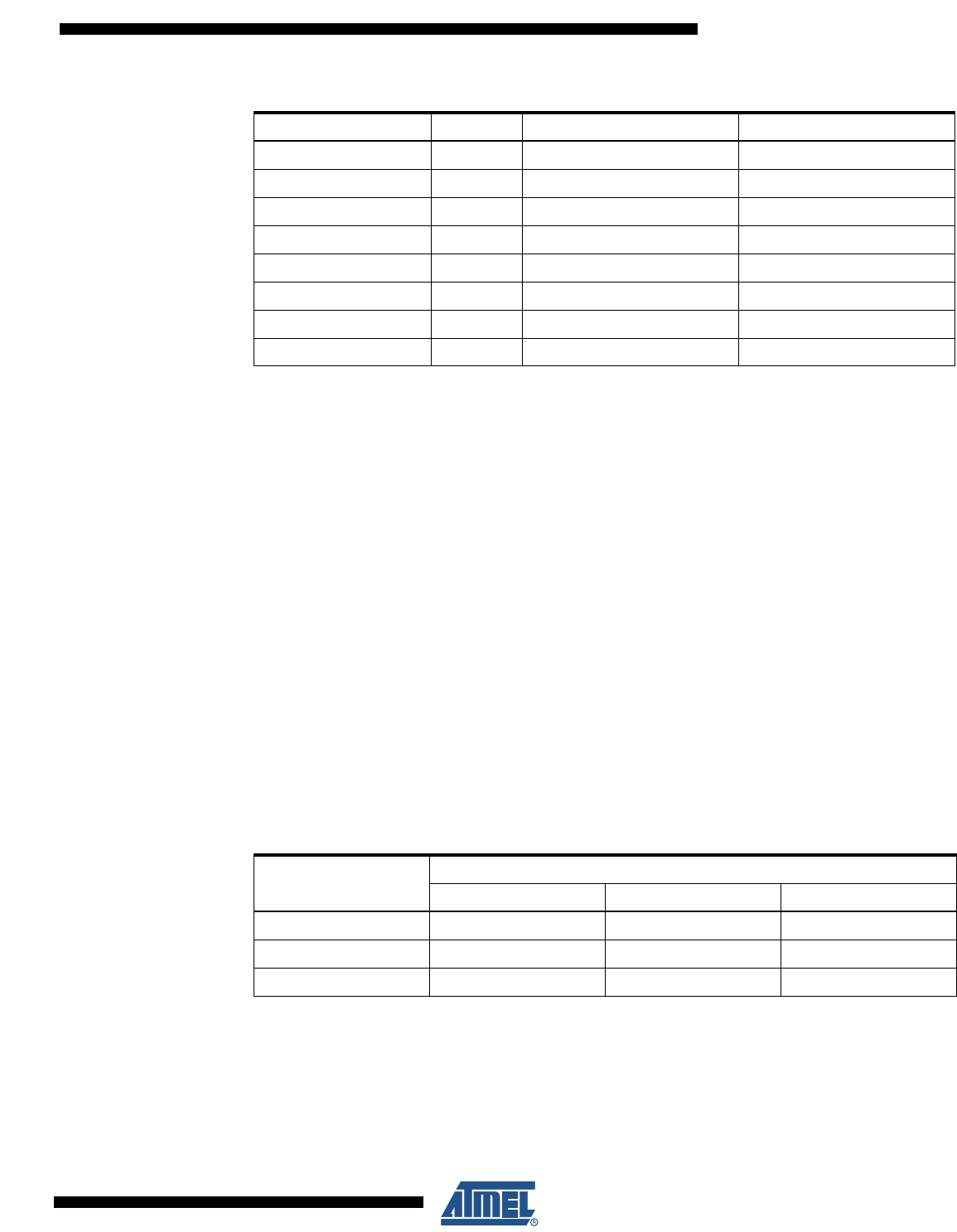
Table 27-7. Fuse Low Byte
Low Fuse Byte Bit No Description Default Value
CKDIV8
(4)
7 Divide clock by 8 0 (programmed)
CKOUT
(3)
6 Clock output 1 (unprogrammed)
SUT1 5 Select start-up time 1 (unprogrammed)
(1)
SUT0 4 Select start-up time 0 (programmed)
(1)
CKSEL3 3 Select Clock source 0 (programmed)
(2)
CKSEL2 2 Select Clock source 0 (programmed)
(2)
CKSEL1 1 Select Clock source 1 (unprogrammed)
(2)
CKSEL0 0 Select Clock source 0 (programmed)
(2)
Table 27-8. Device ID
Part
Signature Bytes Address
0x000 0x001 0x002
ATmega48 0x1E 0x92 0x05
ATmega88 0x1E 0x93 0x0A
ATmega168 0x1E 0x94 0x06
290
2545M–AVR–09/07
ATmega48/88/168
27.5 Page Size
27.6 Parallel Programming Parameters, Pin Mapping, and Commands
This section describes how to parallel program and verify Flash Program memory, EEPROM
Data memory, Memory Lock bits, and Fuse bits in the ATmega48/88/168. Pulses are assumed
to be at least 250 ns unless otherwise noted.
27.6.1 Signal Names
In this section, some pins of the ATmega48/88/168 are referenced by signal names describing
their functionality during parallel programming, see Figure 27-1 and Table 27-11. Pins not
described in the following table are referenced by pin names.
The XA1/XA0 pins determine the action executed when the XTAL1 pin is given a positive pulse.
The bit coding is shown in Table 27-13.
When pulsing WR
or OE, the command loaded determines the action executed. The different
Commands are shown in Table 27-14.
Table 27-9. No. of Words in a Page and No. of Pages in the Flash
Device Flash Size Page Size PCWORD
No. of
Pages PCPAGE PCMSB
ATmega48
2K words
(4K bytes)
32 words PC[4:0] 64 PC[10:5] 10
ATmega88
4K words
(8K bytes)
32 words PC[4:0] 128 PC[11:5] 11
ATmega168
8K words
(16K bytes)
64 words PC[5:0] 128 PC[12:6] 12
Table 27-10. No. of Words in a Page and No. of Pages in the EEPROM
Device
EEPROM
Size
Page
Size PCWORD
No. of
Pages PCPAGE EEAMSB
ATmega48 256 bytes 4 bytes EEA[1:0] 64 EEA[7:2] 7
ATmega88 512 bytes 4 bytes EEA[1:0] 128 EEA[8:2] 8
ATmega168 512 bytes 4 bytes EEA[1:0] 128 EEA[8:2] 8
291
2545M–AVR–09/07
ATmega48/88/168
Figure 27-1. Parallel Programming
Note: V
CC
- 0.3V < AV
CC
< V
CC
+ 0.3V, however, AV
CC
should always be within 4.5 - 5.5V
Table 27-11. Pin Name Mapping
Signal Name in
Programming Mode Pin Name I/O Function
RDY/BSY PD1 O
0: Device is busy programming, 1: Device is
ready for new command
OE
PD2 I Output Enable (Active low)
WR
PD3 I Write Pulse (Active low)
BS1 PD4 I
Byte Select 1 (“0” selects Low byte, “1” selects
High byte)
XA0 PD5 I XTAL Action Bit 0
XA1 PD6 I XTAL Action Bit 1
PAG EL PD 7 I
Program memory and EEPROM Data Page
Load
BS2 PC2 I
Byte Select 2 (“0” selects Low byte, “1” selects
2’nd High byte)
DATA {PC[1:0]: PB[5:0]} I/O Bi-directional Data bus (Output when OE is low)
Table 27-12. Pin Values Used to Enter Programming Mode
Pin Symbol Value
PAGEL Prog_enable[3] 0
XA1 Prog_enable[2] 0
XA0 Prog_enable[1] 0
BS1 Prog_enable[0] 0
VCC
GND
XTAL1
PD1
PD2
PD3
PD4
PD5
PD6
PC[1:0]:PB[5:0]
DATA
RESET
PD7
+12 V
BS1
XA0
XA1
OE
RDY/BSY
PAGEL
PC2
WR
BS2
AVCC
+4.5 - 5.5V
+4.5 - 5.5V
PREVIOUS90919293949596979899100101102103NEXT