Freelance Electronics Components Distributor
Closed Dec 25th-26th
800-300-1968
We Stock Hard to Find Parts

ATMEGA48-20AU

Part # ATMEGA48-20AU
Description MCU 8BIT ATMEGA RISC 4KB FLASH 3.3V/5V 32TQFP - Trays
Category IC
Availability Out of Stock
Qty 0
Qty Price
1 + $1.49230


Technical Document


DISCLAIMER: The information provided herein is solely for informational purposes. Customers must be aware of the suitability of this product for their application, and consider that variable factors such as Manufacturer, Product Category, Date Codes, Pictures and Descriptions may differ from available inventory.

286
2545M–AVR–09/07
ATmega48/88/168
27. Memory Programming
27.1 Program And Data Memory Lock Bits
The ATmega88/168 provides six Lock bits which can be left unprogrammed (“1”) or can be pro-
grammed (“0”) to obtain the additional features listed in Table 27-2. The Lock bits can only be
erased to “1” with the Chip Erase command.The ATmega48 has no separate Boot Loader sec-
tion. The SPM instruction is enabled for the whole Flash if the SELFPRGEN fuse is programmed
(“0”), otherwise it is disabled.
Notes: 1. “1” means unprogrammed, “0” means programmed
2. Only on ATmega88/168.
Notes: 1. Program the Fuse bits and Boot Lock bits before programming the LB1 and LB2.
2. “1” means unprogrammed, “0” means programmed
Table 27-1. Lock Bit Byte
(1)
Lock Bit Byte Bit No Description Default Value
7 1 (unprogrammed)
6 1 (unprogrammed)
BLB12
(2)
5 Boot Lock bit 1 (unprogrammed)
BLB11
(2)
4 Boot Lock bit 1 (unprogrammed)
BLB02
(2)
3 Boot Lock bit 1 (unprogrammed)
BLB01
(2)
2 Boot Lock bit 1 (unprogrammed)
LB2 1 Lock bit 1 (unprogrammed)
LB1 0 Lock bit 1 (unprogrammed)
Table 27-2. Lock Bit Protection Modes
(1)(2)
Memory Lock Bits Protection Type
LB Mode LB2 LB1
1 1 1 No memory lock features enabled.
210
Further programming of the Flash and EEPROM is disabled in
Parallel and Serial Programming mode. The Fuse bits are
locked in both Serial and Parallel Programming mode.
(1)
300
Further programming and verification of the Flash and EEPROM
is disabled in Parallel and Serial Programming mode. The Boot
Lock bits and Fuse bits are locked in both Serial and Parallel
Programming mode.
(1)
287
2545M–AVR–09/07
ATmega48/88/168
Notes: 1. Program the Fuse bits and Boot Lock bits before programming the LB1 and LB2.
2. “1” means unprogrammed, “0” means programmed
27.2 Fuse Bits
The ATmega48/88/168 has three Fuse bytes. Table 27-4 - Table 27-7 describe briefly the func-
tionality of all the fuses and how they are mapped into the Fuse bytes. Note that the fuses are
read as logical zero, “0”, if they are programmed.
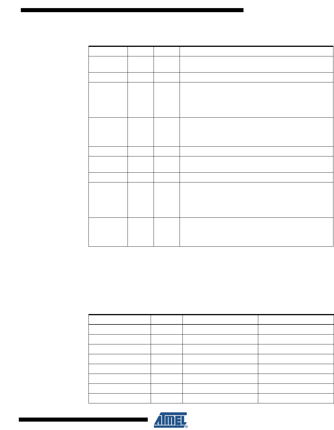
Table 27-3. Lock Bit Protection Modes
(1)(2)
. Only ATmega88/168.
BLB0 Mode BLB02 BLB01
111
No restrictions for SPM or LPM accessing the Application
section.
2 1 0 SPM is not allowed to write to the Application section.
300
SPM is not allowed to write to the Application section, and LPM
executing from the Boot Loader section is not allowed to read
from the Application section. If Interrupt Vectors are placed in
the Boot Loader section, interrupts are disabled while executing
from the Application section.
401
LPM executing from the Boot Loader section is not allowed to
read from the Application section. If Interrupt Vectors are placed
in the Boot Loader section, interrupts are disabled while
executing from the Application section.
BLB1 Mode BLB12 BLB11
111
No restrictions for SPM or LPM accessing the Boot Loader
section.
2 1 0 SPM is not allowed to write to the Boot Loader section.
300
SPM is not allowed to write to the Boot Loader section, and LPM
executing from the Application section is not allowed to read
from the Boot Loader section. If Interrupt Vectors are placed in
the Application section, interrupts are disabled while executing
from the Boot Loader section.
401
LPM executing from the Application section is not allowed to
read from the Boot Loader section. If Interrupt Vectors are
placed in the Application section, interrupts are disabled while
executing from the Boot Loader section.
Table 27-4. Extended Fuse Byte for mega48
Extended Fuse Byte Bit No Description Default Value
–7 1
–6 1
–5 1
–4 1
–3 1
–2 1
–1 1
SELFPRGEN 0 Self Programming Enable 1 (unprogrammed)
288
2545M–AVR–09/07
ATmega48/88/168
Note: 1. The default value of BOOTSZ1..0 results in maximum Boot Size. See Table 27-11 on page
291 for details.
Notes: 1. See “Alternate Functions of Port C” on page 82 for description of RSTDISBL Fuse.
2. The SPIEN Fuse is not accessible in serial programming mode.
3. See “WDTCSR – Watchdog Timer Control Register” on page 54 for details.
4. See Table 28-4 on page 308 for BODLEVEL Fuse decoding.
Table 27-5. Extended Fuse Byte for mega88/168
Extended Fuse Byte Bit No Description Default Value
–7 1
–6 1
–5 1
–4 1
–3 1
BOOTSZ1 2
Select Boot Size
(see Table 26-6 on page 282
and Table 26-9 on page 283
for details)
0 (programmed)
(1)
BOOTSZ0 1
Select Boot Size
(see Table 26-6 on page 282
and Table 26-9 on page 283
for details)
0 (programmed)
(1)
BOOTRST 0 Select Reset Vector 1 (unprogrammed)
Table 27-6. Fuse High Byte
High Fuse Byte Bit No Description Default Value
RSTDISBL
(1)
7 External Reset Disable 1 (unprogrammed)
DWEN 6 debugWIRE Enable 1 (unprogrammed)
SPIEN
(2)
5
Enable Serial Program and
Data Downloading
0 (programmed, SPI
programming enabled)
WDTON
(3)
4 Watchdog Timer Always On 1 (unprogrammed)
EESAVE 3
EEPROM memory is
preserved through the Chip
Erase
1 (unprogrammed), EEPROM
not reserved
BODLEVEL2
(4)
2
Brown-out Detector trigger
level
1 (unprogrammed)
BODLEVEL1
(4)
1
Brown-out Detector trigger
level
1 (unprogrammed)
BODLEVEL0
(4)
0
Brown-out Detector trigger
level
1 (unprogrammed)
PREVIOUS8990919293949596979899100101102NEXT