Freelance Electronics Components Distributor
Closed Dec 25th-26th
800-300-1968
We Stock Hard to Find Parts

ATMEGA48-20AU

Part # ATMEGA48-20AU
Description MCU 8BIT ATMEGA RISC 4KB FLASH 3.3V/5V 32TQFP - Trays
Category IC
Availability Out of Stock
Qty 0
Qty Price
1 + $1.49230


Technical Document


DISCLAIMER: The information provided herein is solely for informational purposes. Customers must be aware of the suitability of this product for their application, and consider that variable factors such as Manufacturer, Product Category, Date Codes, Pictures and Descriptions may differ from available inventory.

247
2545M–AVR–09/07
ATmega48/88/168
read, neither register is updated and the result from the conversion is lost. When ADCH is read,
ADC access to the ADCH and ADCL Registers is re-enabled.
The ADC has its own interrupt which can be triggered when a conversion completes. When ADC
access to the Data Registers is prohibited between reading of ADCH and ADCL, the interrupt
will trigger even if the result is lost.
23.3 Starting a Conversion
A single conversion is started by disabling the Power Reduction ADC bit, PRADC, in “Minimizing
Power Consumption” on page 42 by writing a logical zero to it and writing a logical one to the
ADC Start Conversion bit, ADSC. This bit stays high as long as the conversion is in progress
and will be cleared by hardware when the conversion is completed. If a different data channel is
selected while a conversion is in progress, the ADC will finish the current conversion before per-
forming the channel change.
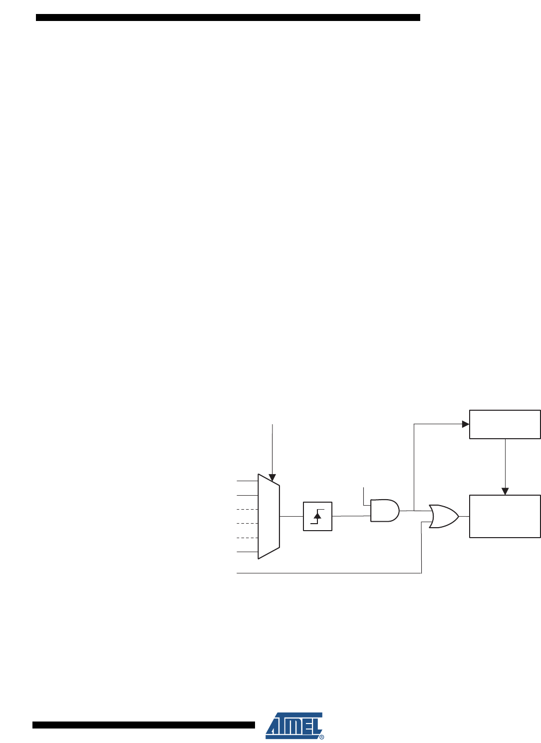
Alternatively, a conversion can be triggered automatically by various sources. Auto Triggering is
enabled by setting the ADC Auto Trigger Enable bit, ADATE in ADCSRA. The trigger source is
selected by setting the ADC Trigger Select bits, ADTS in ADCSRB (See description of the ADTS
bits for a list of the trigger sources). When a positive edge occurs on the selected trigger signal,
the ADC prescaler is reset and a conversion is started. This provides a method of starting con-
versions at fixed intervals. If the trigger signal still is set when the conversion completes, a new
conversion will not be started. If another positive edge occurs on the trigger signal during con-
version, the edge will be ignored. Note that an Interrupt Flag will be set even if the specific
interrupt is disabled or the Global Interrupt Enable bit in SREG is cleared. A conversion can thus
be triggered without causing an interrupt. However, the Interrupt Flag must be cleared in order to
trigger a new conversion at the next interrupt event.
Figure 23-2. ADC Auto Trigger Logic
Using the ADC Interrupt Flag as a trigger source makes the ADC start a new conversion as soon
as the ongoing conversion has finished. The ADC then operates in Free Running mode, con-
stantly sampling and updating the ADC Data Register. The first conversion must be started by
writing a logical one to the ADSC bit in ADCSRA. In this mode the ADC will perform successive
conversions independently of whether the ADC Interrupt Flag, ADIF is cleared or not.
A
DSC
ADIF
SOURCE 1
SOURCE n
ADTS[2:0]
CONVERSION
LOGIC
PRESCALER
START
CLK
ADC
.
.
.
.
EDGE
DETECTOR
ADATE
248
2545M–AVR–09/07
ATmega48/88/168
If Auto Triggering is enabled, single conversions can be started by writing ADSC in ADCSRA to
one. ADSC can also be used to determine if a conversion is in progress. The ADSC bit will be
read as one during a conversion, independently of how the conversion was started.
23.4 Prescaling and Conversion Timing
Figure 23-3. ADC Prescaler
By default, the successive approximation circuitry requires an input clock frequency between 50
kHz and 200 kHz to get maximum resolution. If a lower resolution than 10 bits is needed, the
input clock frequency to the ADC can be higher than 200 kHz to get a higher sample rate.
The ADC module contains a prescaler, which generates an acceptable ADC clock frequency
from any CPU frequency above 100 kHz. The prescaling is set by the ADPS bits in ADCSRA.
The prescaler starts counting from the moment the ADC is switched on by setting the ADEN bit
in ADCSRA. The prescaler keeps running for as long as the ADEN bit is set, and is continuously
reset when ADEN is low.
When initiating a single ended conversion by setting the ADSC bit in ADCSRA, the conversion
starts at the following rising edge of the ADC clock cycle.
A normal conversion takes 13 ADC clock cycles. The first conversion after the ADC is switched
on (ADEN in ADCSRA is set) takes 25 ADC clock cycles in order to initialize the analog circuitry.
When the bandgap reference voltage is used as input to the ADC, it will take a certain time for
the voltage to stabilize. If not stabilized, the first value read after the first conversion may be
wrong.
The actual sample-and-hold takes place 1.5 ADC clock cycles after the start of a normal conver-
sion and 13.5 ADC clock cycles after the start of an first conversion. When a conversion is
complete, the result is written to the ADC Data Registers, and ADIF is set. In Single Conversion
mode, ADSC is cleared simultaneously. The software may then set ADSC again, and a new
conversion will be initiated on the first rising ADC clock edge.
When Auto Triggering is used, the prescaler is reset when the trigger event occurs. This assures
a fixed delay from the trigger event to the start of conversion. In this mode, the sample-and-hold
takes place two ADC clock cycles after the rising edge on the trigger source signal. Three addi-
tional CPU clock cycles are used for synchronization logic.
7-BIT ADC PRESCALER
ADC CLOCK SOURCE
CK
ADPS0
ADPS1
ADPS2
CK/128
CK/2
CK/4
CK/8
CK/16
CK/32
CK/64
Reset
A
DEN
S
TART
249
2545M–AVR–09/07
ATmega48/88/168
In Free Running mode, a new conversion will be started immediately after the conversion com-
pletes, while ADSC remains high. For a summary of conversion times, see Table 23-1 on page
250.
Figure 23-4. ADC Timing Diagram, First Conversion (Single Conversion Mode)
Figure 23-5. ADC Timing Diagram, Single Conversion
Figure 23-6. ADC Timing Diagram, Auto Triggered Conversion
Sign and MSB of Result
LSB of Result
ADC Clock
ADSC
Sample & Hold
ADIF
ADCH
ADCL
Cycle Number
ADEN
1 212
13
14 15
16 17
18 19 20 21 22 23
24 25
1 2
First Conversion
Next
Conversion
3
MUX and REFS
Update
MUX and REFS
Update
Conversion
Complete
1
2 3 4 5 6 7 8
9 10 11 12 13
Sign and MSB of Result
LSB of Result
ADC Clock
ADSC
ADIF
ADCH
ADCL
Cycle Number
12
One Conversion Next Conversion
3
Sample & Hold
MUX and REFS
Update
Conversion
Complete
MUX and REFS
Update
1 2 3 4 5 6 7 8
9
10 11 12 13
Sign and MSB of Result
LSB of Result
ADC Clock
Trigger
Source
ADIF
ADCH
ADCL
Cycle Number
12
One Conversion Next Conversion
Conversion
Complete
Prescaler
Reset
ADATE
Prescaler
Reset
Sample &
Hold
MUX and REFS
Update
PREVIOUS7677787980818283848586878889NEXT