Freelance Electronics Components Distributor
Closed Dec 25th-26th
800-300-1968
We Stock Hard to Find Parts

ATMEGA48-20AU

Part # ATMEGA48-20AU
Description MCU 8BIT ATMEGA RISC 4KB FLASH 3.3V/5V 32TQFP - Trays
Category IC
Availability Out of Stock
Qty 0
Qty Price
1 + $1.49230


Technical Document


DISCLAIMER: The information provided herein is solely for informational purposes. Customers must be aware of the suitability of this product for their application, and consider that variable factors such as Manufacturer, Product Category, Date Codes, Pictures and Descriptions may differ from available inventory.

241
2545M–AVR–09/07
ATmega48/88/168
Figure 21-22. TWI Address Match Logic, Block Diagram
Bit 0 – Res: Reserved Bit
This bit is an unused bit in the ATmega48/88/168, and will always read as zero.
Addre
ss
Match
Address Bit Comparator 0
Address Bit Comparator 6..1
TWAR0
TWAMR0
Address
Bit 0
242
2545M–AVR–09/07
ATmega48/88/168
22. Analog Comparator
22.1 Overview
The Analog Comparator compares the input values on the positive pin AIN0 and negative pin
AIN1. When the voltage on the positive pin AIN0 is higher than the voltage on the negative pin
AIN1, the Analog Comparator output, ACO, is set. The comparator’s output can be set to trigger
the Timer/Counter1 Input Capture function. In addition, the comparator can trigger a separate
interrupt, exclusive to the Analog Comparator. The user can select Interrupt triggering on com-
parator output rise, fall or toggle. A block diagram of the comparator and its surrounding logic is
shown in Figure 22-1.
The Power Reduction ADC bit, PRADC, in “Minimizing Power Consumption” on page 42 must
be disabled by writing a logical zero to be able to use the ADC input MUX.
Figure 22-1. Analog Comparator Block Diagram
(2)
Notes: 1. See Table 22-1 on page 242.
2. Refer to Figure 1-1 on page 2 and Table 13-9 on page 85 for Analog Comparator pin
placement.
22.2 Analog Comparator Multiplexed Input
It is possible to select any of the ADC7..0 pins to replace the negative input to the Analog Com-
parator. The ADC multiplexer is used to select this input, and consequently, the ADC must be
switched off to utilize this feature. If the Analog Comparator Multiplexer Enable bit (ACME in
ADCSRB) is set and the ADC is switched off (ADEN in ADCSRA is zero), MUX2..0 in ADMUX
select the input pin to replace the negative input to the Analog Comparator, as shown in Table
22-1. If ACME is cleared or ADEN is set, AIN1 is applied to the negative input to the Analog
Comparator.
ACBG
BANDGAP
REFERENCE
ADC MULTIPLEXER
OUTPUT
ACME
ADEN
(1)
Table 22-1. Analog Comparator Multiplexed Input
ACME ADEN MUX2..0 Analog Comparator Negative Input
0 x xxx AIN1
1 1 xxx AIN1
1 0 000 ADC0
243
2545M–AVR–09/07
ATmega48/88/168
22.3 Register Description
22.3.1 ADCSRB – ADC Control and Status Register B
Bit 6 – ACME: Analog Comparator Multiplexer Enable
When this bit is written logic one and the ADC is switched off (ADEN in ADCSRA is zero), the
ADC multiplexer selects the negative input to the Analog Comparator. When this bit is written
logic zero, AIN1 is applied to the negative input of the Analog Comparator. For a detailed
description of this bit, see Analog Comparator Multiplexed Input” on page 242.
22.3.2 ACSR – Analog Comparator Control and Status Register
Bit 7 – ACD: Analog Comparator Disable
When this bit is written logic one, the power to the Analog Comparator is switched off. This bit
can be set at any time to turn off the Analog Comparator. This will reduce power consumption in
Active and Idle mode. When changing the ACD bit, the Analog Comparator Interrupt must be
disabled by clearing the ACIE bit in ACSR. Otherwise an interrupt can occur when the bit is
changed.
Bit 6 – ACBG: Analog Comparator Bandgap Select
When this bit is set, a fixed bandgap reference voltage replaces the positive input to the Analog
Comparator. When this bit is cleared, AIN0 is applied to the positive input of the Analog Compar-
ator. When the bandgap reference voltage is used as input to the Analog Comparator, it will take
a certain time for the voltage to stabilize. If not stabilized, the first conversion may give a wrong
value. See “Internal Voltage Reference” on page 49
Bit 5 – ACO: Analog Comparator Output
The output of the Analog Comparator is synchronized and then directly connected to ACO. The
synchronization introduces a delay of 1 - 2 clock cycles.
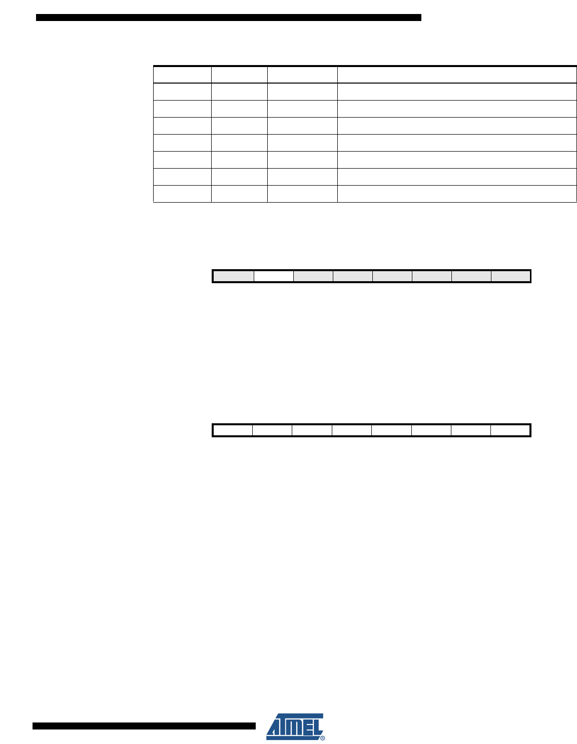
1 0 001 ADC1
1 0 010 ADC2
1 0 011 ADC3
1 0 100 ADC4
1 0 101 ADC5
1 0 110 ADC6
1 0 111 ADC7
Table 22-1. Analog Comparator Multiplexed Input (Continued)
ACME ADEN MUX2..0 Analog Comparator Negative Input
Bit 76543210
(0x7B)
–ACME ADTS2 ADTS1 ADTS0 ADCSRB
Read/Write R R/W R R R R/W R/W R/W
Initial Value0 0000000
Bit 76543210
0x30 (0x50) ACD ACBG ACO ACI ACIE ACIC ACIS1 ACIS0 ACSR
Read/Write R/W R/W R R/W R/W R/W R/W R/W
Initial Value 0 0 N/A 0 0 0 0 0
PREVIOUS7475767778798081828384858687NEXT